Gan Hemt Fabrication Process
Gallium nitride is a semiconductor compound commonly used in lightemitting diodes (LEDs) The material has the ability to conduct electrons more than 1,000 times more efficiently than silicon.

Gan hemt fabrication process. GaNbased highelectronmobility transistors (HEMTs) are fabricated on Gapolar GaN This device is called a Gapolar GaN HEMT Recently, the Npolar GaN=Al xGa 1−xN=GaN HEMT has attracted much attention because its back barrier can strongly confine electrons at the upper side of the GaN= Al xGa 1−xN heterointerface 3,4) Thus, the Al xGa 1−xN layer acts. 13 IEEE Compound Semiconductor Integrated Circuit Symposium (CSICS) We report on a novel fabrication process of GaNonDiamond high electron mobility transistors (HEMTs) and its resulting thermal performance enhancement over conventional GaNonSiC technology In this process, GaN devices are first fabricated on their epitaxial substrate (eg sapphire or SiC) before being removed from the original substrate and bonded onto a highthermalconductivity diamond substrate at low temperature. Usually GaN layers are deposited using Metal Organic Chemical Vapor Deposition (MOCVD) or Molecular Beam Epitaxy (MBE) GaN can be deposited on several types of substrates such as Sapphire, Silicon or Silicon Carbide (SiC), but the cost of GaN epi process and repeatable highquality crystal growth are challenges in GaNbased device fabrication.
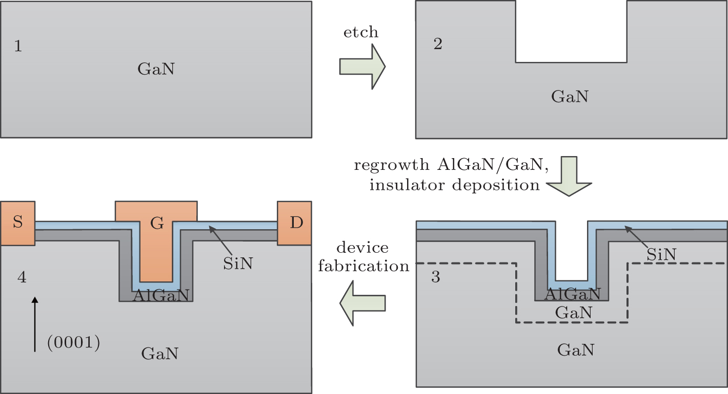
Fig1 Schematic crosssection of fabricated AlGaN/GaN HEMT The fabrication process began with mesa isolation by Cl2/Ar electron cyclotron resonance reactive ion beam etching (ECRRIBE) After the mesaisolation, Ti/Al were evaporated by Ebeam and annealed by RTA in N2 ambient to form source and drain electrodes. Metalorganic chemical vapor depositiongrown fieldplated 025μm gatelength AlGaN/GaN highelectron mobility transistors (HEMTs) with fieldplate lengths of 05, 08, and 11 μm have been. Usually GaN layers are deposited using Metal Organic Chemical Vapor Deposition (MOCVD) or Molecular Beam Epitaxy (MBE) GaN can be deposited on several types of substrates such as Sapphire, Silicon or Silicon Carbide (SiC), but the cost of GaN epi process and repeatable highquality crystal growth are challenges in GaNbased device fabrication.
FABRICATION, MODELING AND CHARACTERIZATION OF GaN HEMTs, AND DESIGN OF HIGH POWER MMIC AMPLIFIERS A THESIS GaAs pHEMT process of UMS foundry We introduced twostage balanced PA topology in order to achieve wideband and high power response at the output. FABRICATION AND CHARACTERIZATION OF SUBMICRON ALGAN/GAN HEMTS V Desmaris, J Eriksson, N Rorsman, H Zirath CONCLUSION AlGaN/GaN HEMTs, with total gate periphery of 06 mm were successfully fabricated with our inhouse 03 µm process flow on commercial wafers Output drain current densities over 1 A/mm were measured. Voltage GaN HEMT WeiJia Zhang Master of Applied Science Graduate Department of Electrical and Computer Engineering University of Toronto 15 Abstract GaNbased power electronics receive many interests because of its wider bandgap, higher electron mobility and higher critical electrical field than silicon.
Gallium nitride (GaN) technology continues to evolve, pushing the limits of what’s possible with everincreasing power density, reliability and gain in a reduced size No longer a technology just for defense/aerospace applications,. Investigation with very detail to optimize the design, fabrication process, and electronic properties to realize AlInN/GaN HEMTs Each single step of this process was optimized in order to improve device performance The work started with establishing the main features of AlInN/GaN. One of the challenges in GaN power device fabrication is to achieve a “normally off” operation While AlGaN/GaN High Electron Mobility Transistors (HEMT) devices are generally “normally on” and require a circuit to turn off the devices, a normallyoff operation is preferred for safety concerns.
The CMPA601C025D is a GIN1 EMTbased integrated circuit with 05 nm high electron mobility transistors and a metal Tgate that can be used for highspeed trains (see FIG) The semiconductor device (400 nm) belongs to a group of semiconductors consisting of highpower transistors (HemT) that form the basis for an energysaving, lowpower, low. The epitaxial layers were grown on a 2in Si (111) substrate by MOCVD After the preparation of the epitaxial wafer, the normallyoff pGaN/AlGaN/GaN HEMT on a Si substrate was achieved by hydrogen plasma treatment The main structure of the epitaxial wafer includes a 1 µm GaN buffer layer, a 100 nm GaN channel layer, a 1 nm AlN spacer layer, an 18 nm undoped Al 02 Ga 08 N barrier layer. The experimental data on the plasma etching of Si3N4 for sub100 nm gate fabrication for high electron mobility transistors (HEMTs) based on InAlN/GaN heterostructures are analyzed.
FABRICATION, MODELING AND CHARACTERIZATION OF GaN HEMTs, AND DESIGN OF HIGH POWER MMIC AMPLIFIERS A THESIS GaAs pHEMT process of UMS foundry We introduced twostage balanced PA topology in order to achieve wideband and high power response at the output. Abstract A novel early gate dielectric AlGaN/GaN metalinsulatorsemiconductor highelectronmobility transistors (MISHEMTs) process is reported With the highquality Si 3 N 4 dielectric by lowpressure chemical vapor deposition and damage free, selfterminating passivation layer etching at the gate area, the MISHEMTs on 150mm Si substrate demonstrate excellent output performance and good. A GaNonSapphire HEMT Process Flow Example ③Deposit S/D metal Ø Deposit ohmic contacts on top of AlGaN as source and drain Sapphire Substrate Buffer GaN AlGaN S D ④Liftoff and Anneal Ø To improve contact quality Ø Bad annealing may dramatically degrade the device performance ⑤Mask 03 –Gate Ø Definegateregion Ø.
Fabrication of AlGaN/GaN FinType HEMT Using a Novel TGate Process for Improved RadioFrequency Performance Abstract To increase the radiofrequency (RF) performance of AlGaN/GaNbased fintype high electron mobility transistors (HEMTs), a novel Tgate process was developed and applied to fabricate a device with high RF performance In a single lithography process, the applied Tgate process shows a technique for forming a Tgate using the reactivity difference of several photoresists. Gallium nitride (Ga N) is a binary III/V direct bandgap semiconductor commonly used in blue lightemitting diodes since the 1990s The compound is a very hard material that has a Wurtzite crystal structureIts wide band gap of 34 eV affords it special properties for applications in optoelectronic, highpower and highfrequency devices For example, GaN is the substrate which makes violet (405. Unfortunately, such gatefirst process is hard to implement in GaN HEMT fabrication due to the high temperature annealing (>800 °C) needed for source/drain Ohmic contacts formation Gate degradation and the likelihood of gatetodrain/source shorts caused by the high thermalbudget Ohmic contact formation preclude the direct implementation of.
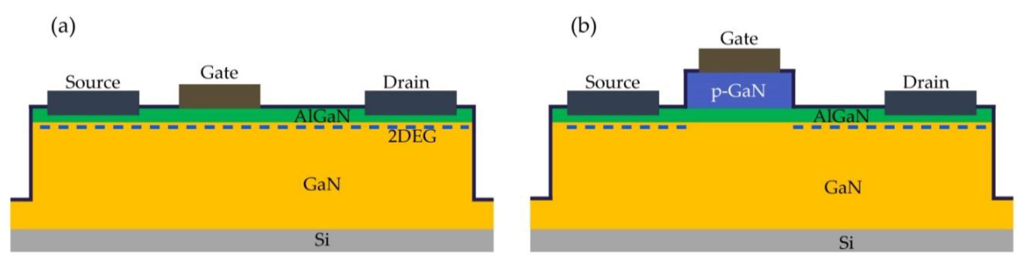
Fig 1 Fabrication process of the AlGaN/GaN HEMT with slant fieldplate structure using deepUV lithography with angle exposure Fig 2 Crosssection profile of Tshaped gate with slant sidewall Fig 3 Power measurement of the AlGaN/GaN HEMT with slant gate at 8 GHz VGS = 15 V, VDS = 50 V 10 Fig 4 RF performance at VDS = 10 V and VGS = 17 V. At present, because of several advantages including simplicity, ease of fabrication, and high transconductance, the Schottkygate (SG) structure is generally used in GaN HEMTs In the high input RF power regime, however, the SG GaN HEMT may suffer from marked leakage currents due to input swings high enough to drive the gate to forward bias 3. The process modules for the GaN HEMT device fabrication include device isolation, pGaN gate formation, contacts for source and drain, contact for gate, surface passivation and so forth In this section, we will focus on some of the key process technologies for the fabrication of pGaN Emode AlGaN/GaN HEMTs, discuss some of the challenges and.
23 Fundamentals of AlGaN/GaN High Electron Mobility Transistors 23 231 AlGaN/GaN HEMT device structure and operating principles 24 232 Formation of 2DEG Channel due to Polarization Effect 27 CHAPTER 3 FABRICATION PROCESS AND CHARACTERIZATION. • Manufacturing process flow • Supply chain evaluation • Manufacturing cost analysis • Estimated sales price Wolfspeed RF GaN HEMT CGHVF Title Wolfspeed CGHVF GaN HEMT Pages 66 Date October 16 Format PDF & Excel file Price Full report EUR 3,290 Wolfspeed (Infineon) offers a broad range of GaN RF products that are. Even at 750 C in a furnace 4, which makes the fabrication of selfaligned devices feasible In this Letter, we report the fabrication and characterisation of selfaligned AlGaN=GaN HEMTs Device fabrication Fig 1 shows the crosssectional view of the selfaligned Tgate AlGaN=GaN HEMT The epilayer of the AlGaN=GaN.
Keywords wide bandgap, GaN, HEMT, nanocrystalline diamond Abstract Diamond has been proposed as an integrated heat sink layer for Gallium Nitride (GaN) high electron mobility transistors (HEMTs) The NRL “Gate after diamond” approach has demonstrated % reduction in selfheating The second generation of this process. On the second part of the dissertation, Aluminum gallium nitride/gallium nitride high electron mobility transistors (AlGaN/GaN HEMTs) were fabricated Round HEMTtechnology, which greatly simplifies the microelectronic fabrication process compared to traditional open fingers HEMT, was employed. Currently GaN high electron mobility transistor (HEMT) technology is under extensive research in both industry and institutes Tinggi Technologies started to development its own HEMT process from 05 This paper evaluates the development of GaN HEMT in past 15 years and the entire fabrication process of Tinggi top GaN HEMT.
AlGaN/GaN high electron mobility transistors (HEMTs) are good candidates for high power, high frequency, and low loss applications because of high critical breakdown field and high electron mobility 9–14 The breakdown voltage (BV) is one of the most important design targets, and the reported values are still far below the theoretical limit. 23 Fundamentals of AlGaN/GaN High Electron Mobility Transistors 23 231 AlGaN/GaN HEMT device structure and operating principles 24 232 Formation of 2DEG Channel due to Polarization Effect 27 CHAPTER 3 FABRICATION PROCESS AND CHARACTERIZATION. Fabrication plan for Power HEMT using field plate Submitted By Vivek Kumar Surana Structure to be used 12 nm Al030Ga070N 10 nm Al2 Ga070 NSi nm Al030 Ga070N 030 1 nm AlN 140nm GaN 042m Al010Ga090N 70 nm Grad up to Al010 Ganm 70 AlN (HT) 090N 3 SiC STEP 1 SiNx passivation 300nm SiNx Technical parameters Deosited by ICPCVD SiH4/N2/Ar=28/9/90sccm Power 0W Pressure 35mTorr.
GaN Transistor Fabrication Process With Liu Zhihong This chapter describes a few key process steps to fabricate GaN highelectronmobility transistors (HEMTs) for power electronics applications The whole process flow to fabricate a HEMT mainly includes five steps, namely mesa isolation, ohmic contact formation, gate formation, pad and. AlGaN/GaN high electron mobility transistors (HEMTs) are good candidates for high power, high frequency, and low loss applications because of high critical breakdown field and high electron mobility 9–14 The breakdown voltage (BV) is one of the most important design targets, and the reported values are still far below the theoretical limit. The reported Aufree AlGaN/GaN HEMT fabrication process can be used in standard Si fabs without the risk of contamination Discover the world's research 17 million members.
• Manufacturing process flow • Supply chain evaluation • Manufacturing cost analysis • Estimated sales price Wolfspeed RF GaN HEMT CGHVF Title Wolfspeed CGHVF GaN HEMT Pages 66 Date October 16 Format PDF & Excel file Price Full report EUR 3,290 Wolfspeed (Infineon) offers a broad range of GaN RF products that are in high. A GaNonSapphire HEMT Process Flow Example ③Deposit S/D metal Ø Deposit ohmic contacts on top of AlGaN as source and drain Sapphire Substrate Buffer GaN AlGaN S D ④Liftoff and Anneal Ø To improve contact quality Ø Bad annealing may dramatically degrade the device performance ⑤Mask 03 –Gate Ø Definegateregion Ø. 21 AlGaN/GaN HEMT fabrication The AlGaN/GaN epiwafer consists of 3 μmthick undoped GaN buffer layer, 150 Å thick undoped Al 025 Ga 075 N layer, and 10 Å thick undoped GaN cap layer Metalorganic Chemical Vapor Deposition (MOCVD) is used to deposit AlGaN/GaN on silicon substrate.
Figure 2 AlGaN/GaN HEMT Structure we can expect the electron mobility of about 00cm2=V s Therefore transistors using these structures like Fig2 are called HEMT(high electron mobility transistor)s However, this HEMT devices are depletionmode devices due to the nature of the AlGaN/GaN heterostructure. Fabrication of gates is the most crucial part in fieldeffect transistor manufacturing due to its strong influence on device performance and reliability Currently, the most commonly used technology for GaNbased HEMTs and MMICs is the socalled “embedded gate” process, where the gate. A GaNonSapphire HEMT Process Flow Example ③Deposit S/D metal Ø Deposit ohmic contacts on top of AlGaN as source and drain Sapphire Substrate Buffer GaN AlGaN S D ④Liftoff and Anneal Ø To improve contact quality Ø Bad annealing may dramatically degrade the device performance ⑤Mask 03 –Gate Ø Definegateregion Ø.
Process development of AlN/GaN MOSHEMTs is presented, along with issues and problems concerning the fabrication processes The developed technology uses thermally grown Al 2 O 3 as a gate dielectric and surface passivation for devices Significant improvement in device performance was observed using the following techniques (1) Ohmic contact optimisation using Al wet etch prior to Ohmic. Process development of AlN/GaN MOSHEMTs is presented, along with issues and problems concerning the fabrication processes The developed technology uses thermally grown Al 2 O 3 as a gate dielectric and surface passivation for devices Significant improvement in device performance was observed using the following techniques (1) Ohmic contact optimisation using Al wet etch prior to Ohmic. The article presents the results of development of selective etching of pGaN over Al 025 Ga 075 N in Cl 2 /Ar/O 2 ICP plasma for fabrication of normallyoff pGaN gate GaN HEMTs using a laser reflectometry system for precise control of the etched material thickness By optimizing etching process parameters such as oxygen flow, ICP power and chamber pressure, high etching selectivity of p.
M S Cho et al Fabrication of AlGaN/GaN FinType HEMT Using a Novel TGate Process for Improved RF Performance FIGURE 3 IDSVGS transfer characteristics of the fabricated AlGaN/GaN fintype HEMT with a Tgate under VDS D 7 V The inset shows the IDSVGS transfer curves and gate leakage current on a logarithmic scale a gate to source length (LGS) of 6 m, and a gate to drain. AlGaN/GaN high electron mobility transistors (HEMTs) are good candidates for high power, high frequency, and low loss applications because of high critical breakdown field and high electron mobility 9–14 The breakdown voltage (BV) is one of the most important design targets, and the reported values are still far below the theoretical limit. GaN HEMT devices are particularly significant in power electronics applications In this thesis, a comprehensive study of normallyoff highelectronmobility transistors is presented, including theoretical background review, theoretical analysis, physicallybased device simulations, device fabrication and optimization and.
A GaNonSapphire HEMT Process Flow Example ③Deposit S/D metal Ø Deposit ohmic contacts on top of AlGaN as source and drain Sapphire Substrate Buffer GaN AlGaN S D ④Liftoff and Anneal Ø To improve contact quality Ø Bad annealing may dramatically degrade the device performance ⑤Mask 03 –Gate Ø Definegateregion Ø. On the second part of the dissertation, Aluminum gallium nitride/gallium nitride high electron mobility transistors (AlGaN/GaN HEMTs) were fabricated Round HEMTtechnology, which greatly simplifies the microelectronic fabrication process compared to traditional open fingers HEMT, was employed. • Demonstrated Advantage of NPolar GaN II The NPolar GaN Deep Recess HEMT • Enabling Features of the Device Structure • Fabrication Process for SelfAligned Gate III Experimental Results Large Signal Performance • WBand Device Performance (94 GHz) • KaBand Device Performance (30 GHz) IV Conclusion.
II FABRICATION CHALLENGES IN HEMT DEVICES 1 GaAs HEMT The most commonly degrading mechanism in GaAs based HEMT device include hot carrier injection mechanism, high mechanical stress, avalanche breakdown in semiconductors 2 GaN HEMT The main challenge of fabricating a GaN HEMT device is the trap generation. The epitaxial layers were grown on a 2in Si (111) substrate by MOCVD After the preparation of the epitaxial wafer, the normallyoff pGaN/AlGaN/GaN HEMT on a Si substrate was achieved by hydrogen plasma treatment The main structure of the epitaxial wafer includes a 1 µm GaN buffer layer, a 100 nm GaN channel layer, a 1 nm AlN spacer layer, an 18 nm undoped Al 02 Ga 08 N barrier layer. Nitronex pioneered AlGaN/GaN HEMTs on commercially available 100mm high resistivity Silicon substrates Since demonstrating the reliability of the Nitronex NRF1 process technology in 06, well over 500,000 units have been shipped worldwide to top tier customers Nitronex has further advanced the manufacturability of AlGaN/GaN HEMTs by successfully transferring the wafer fabrication process to.
To increase the radiofrequency (RF) performance of AlGaN/GaNbased fintype high electron mobility transistors (HEMTs), a novel Tgate process was developed and applied to fabricate a device with high RF performance In a single lithography process, the applied Tgate process shows a technique for forming a Tgate using the reactivity difference of several photoresists The fabricated device. M S Cho et al Fabrication of AlGaN/GaN FinType HEMT Using a Novel TGate Process for Improved RF Performance FIGURE 3 IDSVGS transfer characteristics of the fabricated AlGaN/GaN fintype HEMT with a Tgate under VDS D 7 V The inset shows the IDSVGS transfer curves and gate leakage current on a logarithmic scale a gate to source length (LGS) of 6 m, and a gate to drain. 23 Fundamentals of AlGaN/GaN High Electron Mobility Transistors 23 231 AlGaN/GaN HEMT device structure and operating principles 24 232 Formation of 2DEG Channel due to Polarization Effect 27 CHAPTER 3 FABRICATION PROCESS AND CHARACTERIZATION.
2 Fabrication Fig 1 shows the crosssectional view of selfaligned Tgate AlGaN/GaN HEMT The epilayer of AlGaN/GaN HEMTstructure was grown by metalorganic chemical vapor deposition on (0001) sapphire substrate Theepilayer consists of40nmAINnucleation layer, 3,km of undoped GaN, and nmundoped Al03GaO7N The sheet resistance of. In this paper, the fabrication of an Npolar GaN= Al xGa 1−xN=GaN HEMT on a GaN film with little step bunching is described In this HEMT, the isotropy of the transconductance with respect to the direction of the current flow is shown Other basic characteristics of this HEMT are also reported An Npolar GaN=Al xGa 1−xN=GaN. GaN HEMT devices are particularly significant in power electronics applications In this thesis, a comprehensive study of normallyoff highelectronmobility transistors is presented, including theoretical background review, theoretical analysis, physicallybased device simulations, device fabrication and optimization and.
Gallium nitride (Ga N) is a binary III/V direct bandgap semiconductor commonly used in blue lightemitting diodes since the 1990s The compound is a very hard material that has a Wurtzite crystal structureIts wide band gap of 34 eV affords it special properties for applications in optoelectronic, highpower and highfrequency devices For example, GaN is the substrate which makes violet (405. AlGaN/GaN high electron mobility transistors (HEMTs) have shown outstanding improvements in performance and reliability, becoming the leading option for power applications in the 140 GHz range However, the presence of traps and defects in the heterostructure are strongly correlated to the tolerance of the fabrication process New powerful models designed to overcome limitations associated.
Http Www Jsts Org Html Journal Journal Files 04 Yearvolume 02 07 Pdf
Www Tu Ilmenau De Fileadmin Media Mne Nano Publikationen Jacobs Pssa214 Ic Algan Hemt Jatal Pdf
Transfer Of Algan Gan Rf Devices Onto Diamond Substrates Via Van Der Waals Bonding
Gan Hemt Fabrication Process のギャラリー
A A Schematic Of A Gan Hemt Showing Stress Conditions B Xps Of The Download Scientific Diagram
Publikationen Bibliothek Kit Edu
Scholarcommons Sc Edu Cgi Viewcontent Cgi Article 4657 Context Etd
Development Of 0mm Gan On Si Technology And Power Devices Imec
2
An Effective Hydroxylation Route For A Highly Sensitive Glucose Sensor Using Aptes Gox Functionalized Algan Gan High Electron Mobility Transistor Rsc Advances Rsc Publishing
Http Publications Rwth chen De Record Files Javorka Peter Pdf
2
Mitsubishi Electric Develops World S First Multi Cell Gan Hemt Bonded Directly To Diamond Substrate 19 Globale Neuigkeiten Mitsubishi Electric Deutschland
Q Tbn And9gcr5yaa9idzub4ouuiyyzodc4vgznki8dmenjmdrrbhgxf9ysttf Usqp Cau
Http Www Ep Liu Se Ecp 008 Posters 008 Ecpp Pdf
Iopscience Iop Org Article 10 1149 2 jss Pdf
Gaasmantech Com Digests 10 Papers 11 2 056 Pdf
Www Uni Ulm De Fileadmin Website Uni Ulm Hrem Publications 10 Maier Et Al 10 Testing The Temperature Limits Of Gan Based Hemt Devices Pdf

Revisiting The Seminal Apa Optics Gan Hemt Patent Techinsights
Depositonce Tu Berlin De Bitstream 8721 5 Badawi Nasser Pdf
High Electron Mobility Transistor Wikipedia
2
Tel Archives Ouvertes Fr Tel Document
Myukk Org Sm17 Sm Pdf Sm1678 Pdf
Electronics Free Full Text A Comprehensive Review Of Recent Progress On Gan High Electron Mobility Transistors Devices Fabrication And Reliability Html
Moscap And Hemt Process Flows A Moscap Process Flow N Gan Substrate Download Scientific Diagram
Http Www Semiconductor Today Com Features Pdf Semiconductortoday Feb13 Step Towards Pdf
D Nb Info 34
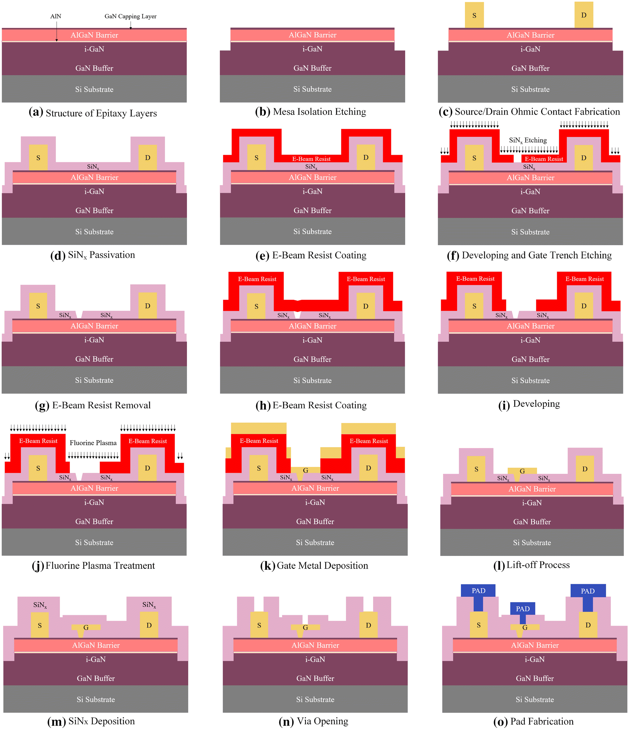
Figure 1 Low Leakage Gan Hemts With Sub 100 Nm T Shape Gates Fabricated By A Low Damage Etching Process Springerlink
Www Wolfspeed Com Downloads Dl File Id 415 Product 130 Cghv1j025d Pdf
1
Iopscience Iop Org Article 10 1149 1 Pdf
Figure 11 Proposal Of A Novel Recess Free Enhancement Mode Algan Gan Hemt With Field Assembled Structure A Simulation Study Springerlink
Http Juser Fz Juelich De Record Files Informationstech 9 Pdf
Elib Uni Stuttgart De Bitstream 116 4808 1 Masterthesis Malik Pdf
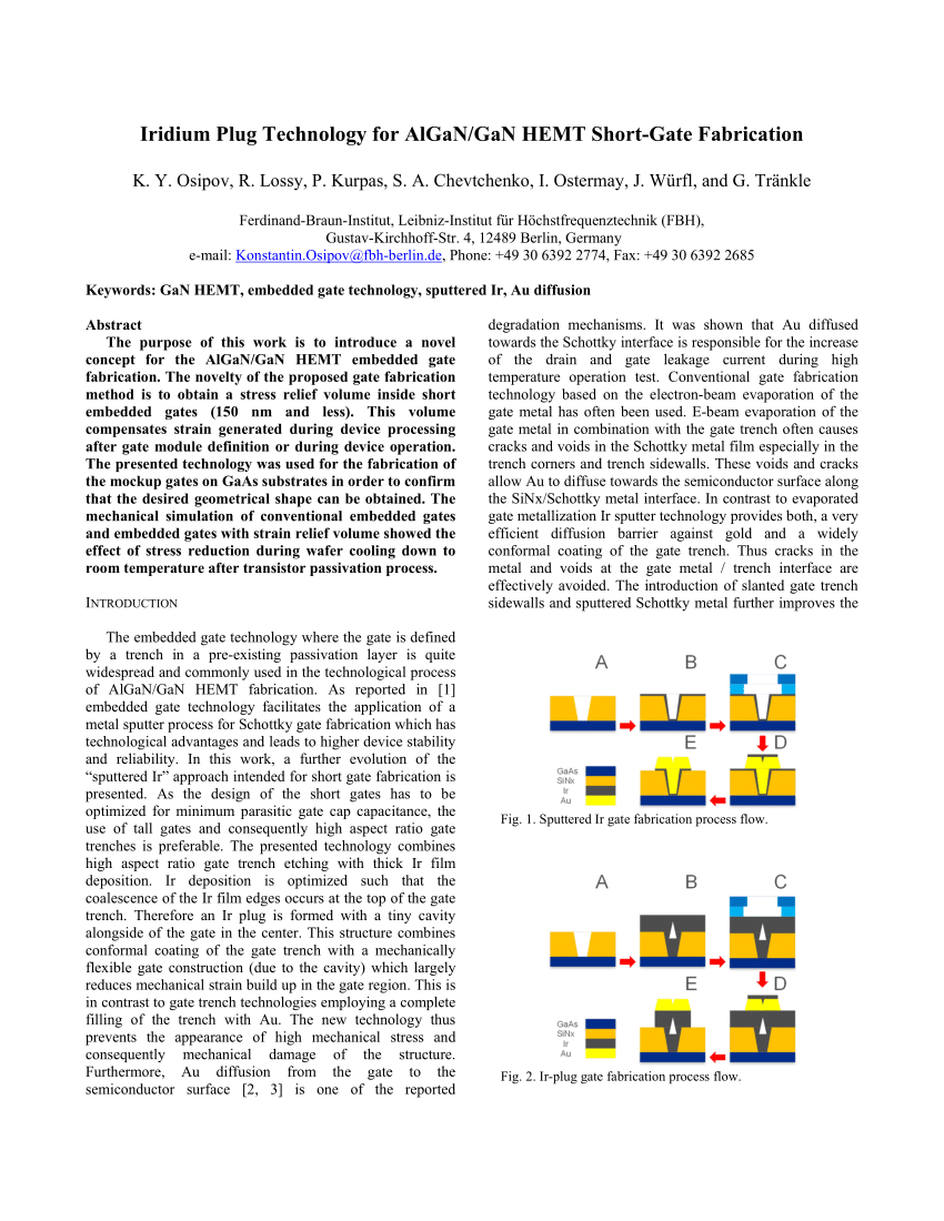
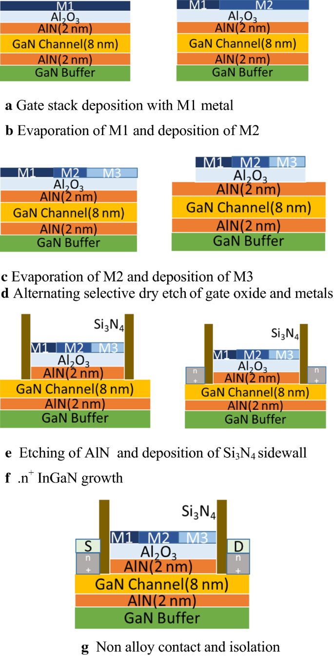
Pdf Iridium Plug Technology For Algan Gan Hemt Short Gate Fabrication
Analytical Model Development Of Channel Potential Electric Field Threshold Voltage And Drain Current For Gate Workfunction Engineered Short Channel E Mode N Polar Gan Mos Hemt Springerlink
2
Electronics Free Full Text A Comprehensive Review Of Recent Progress On Gan High Electron Mobility Transistors Devices Fabrication And Reliability Html
Arxiv Org Pdf 1801
Www Armms Org Media Uploads Pdf
Comparing Gan On Sic Power Transistor Technology With Gaas And Si 5g Technology World
Ieeexplore Ieee Org Iel5 60 296 Pdf
Snfexfab Stanford Edu Sites G Files Sbiybj8726 F Sections Diplayfiles Engr241 Final Report Sj Al 1819win Pdf

Gold Free Contacts On Alxga1 Gan High Electron Mobility Transistor Structure Grown On A 0 Mm Diameter Si 111 Substrate Journal Of Vacuum Science Technology B Vol 34 No 4
Q Tbn And9gcsiwnokh660bsdp8hcogb84hn1iunect0qfrmnl9da Usqp Cau

Sciencecentral
Europractice Ic Com Wp Content Uploads 19 09 Tutorial Allgan Gan Ics Imec Aug19 Pdf
Www Nature Com Articles S 019 3 Pdf Proof T
Www Tu Ilmenau De Fileadmin Media Mne Nano Publikationen Jacobs Pssa214 Emode Dmode Algan Hemt Jatal Pdf
Par Nsf Gov Servlets Purl
2
2

High Performance Ultraviolet Light Detection Using Nano Scale Fin Isolation Algan Gan Heterostructures With Zno Nanorods Abstract Europe Pmc
Snfexfab Stanford Edu Sites G Files Sbiybj8726 F Sections Diplayfiles Engr241 Final Report Sj Al 1819win Pdf
Open Gated Ph Sensor Fabricated On An Undoped Algan Gan Hemt Structure Topic Of Research Paper In Nano Technology Download Scholarly Article Pdf And Read For Free On Cyberleninka Open Science Hub
Www Nature Com Articles S 019 3 Pdf Proof T

Cghv1j070d Datasheet Pdf Datasheet4u Com
2
Gan Hemt Power Device Tcad Simulation Youtube
Characteristics Of Algan Gan High Electron Mobility Transistors On Metallic Substrate
Mitsubishi Electric Develops World S First Multi Cell Gan Hemt Bonded Directly To Diamond Substrate 19 Globale Neuigkeiten Mitsubishi Electric Deutschland
Depositonce Tu Berlin De Bitstream 8721 5 Badawi Nasser Pdf
Http Www Xidian Edu Cn Hyjsktz Docs Pdf

Sciencecentral
Ku Band Algan Gan Hemt With Over 30 Of Pae Manualzz
Core Ac Uk Download Pdf Pdf
2
Cuvillier De Uploads Preview Public File 7437 Pdf

Making Waves With The Gan Hemt News
Http Publications Rwth chen De Record Files Javorka Peter Pdf
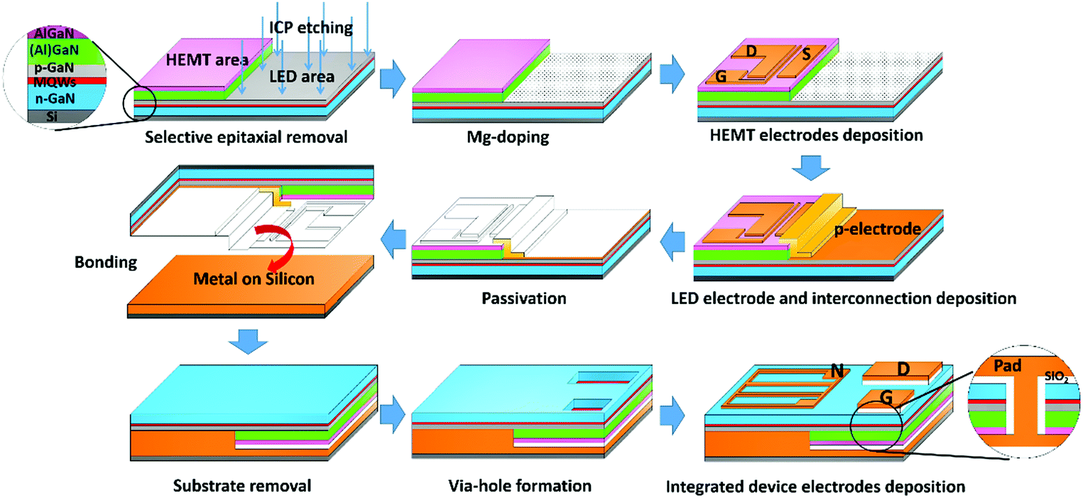
Efficiency Improved By Monolithic Integration Of Hemt With Vertical Structure Leds And Mg Doping On Dry Etched Gan Journal Of Materials Chemistry C Rsc Publishing Doi 10 1039 C9tch

Selective Epitaxial Growth Of Monolithically Integrated Gan Based Light Emitting Diodes With Algan Gan Driving Transistors Applied Physics Letters Vol 104 No 9
Effects Of Gate Shaping And Consequent Process Changes On Algan Gan Hemt Reliability Topic Of Research Paper In Materials Engineering Download Scholarly Article Pdf And Read For Free On Cyberleninka Open Science
Iopscience Iop Org Article 10 10 1361 6463 af9d Pdf
Http Www Jsts Org Html Journal Journal Files 04 Yearvolume 02 07 Pdf
Arxiv Org Pdf 1903
2
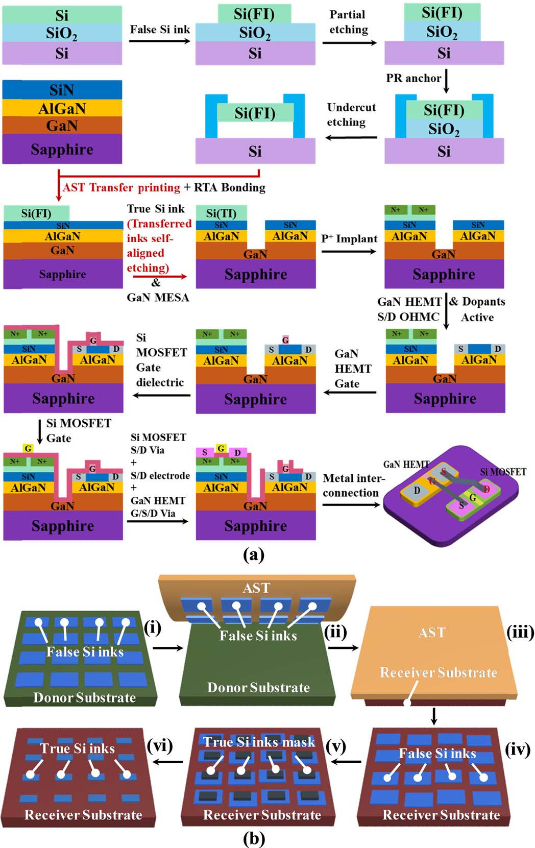
Transfer Printing And Self Aligned Etching For E Mode Gan Transistors

Color Online Flowchart Of Backside Processing Of The Gan Hemt On A Download Scientific Diagram
Www Osti Gov Pages Servlets Purl
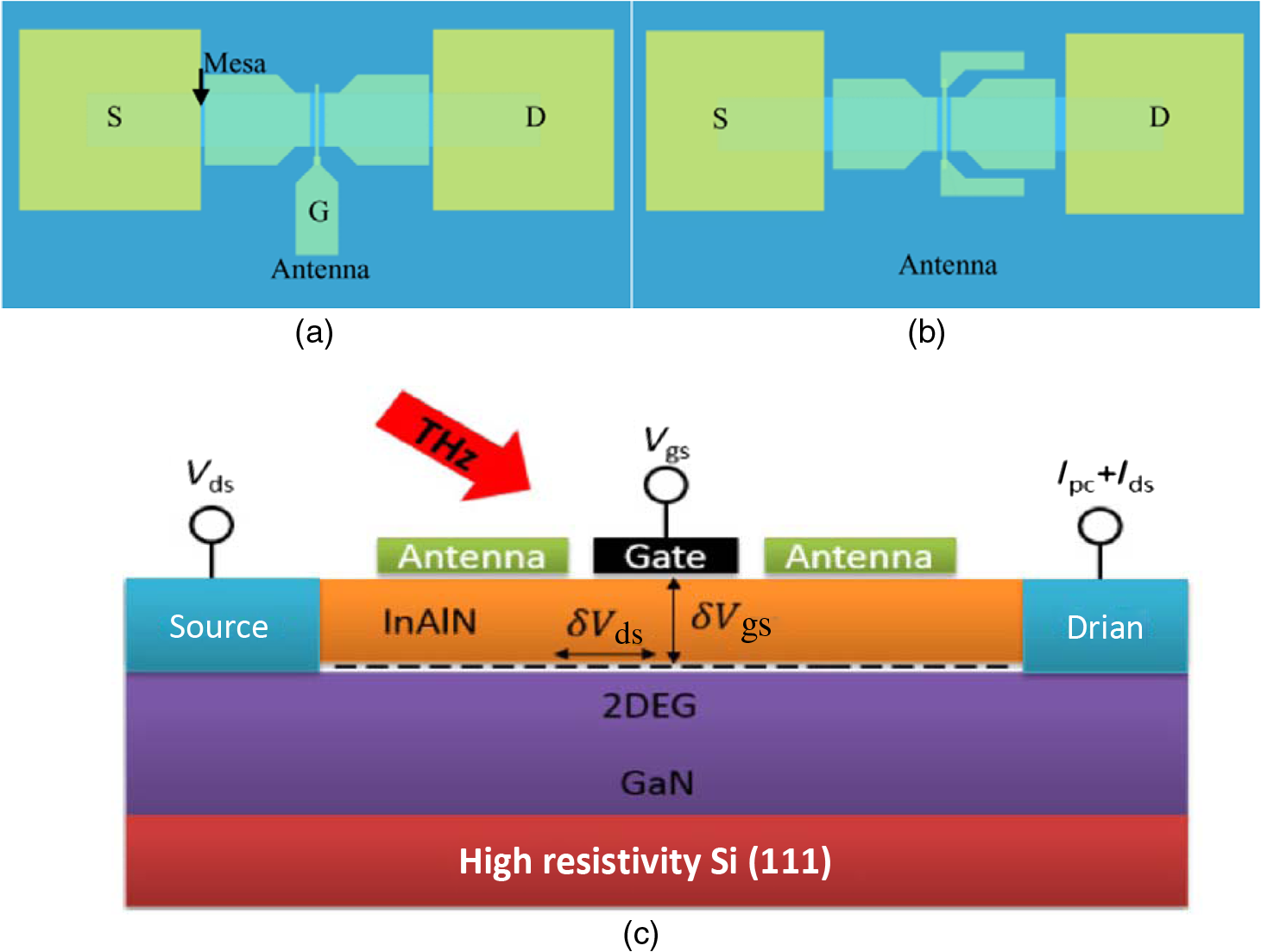
Review Of Gan Based Devices For Terahertz Operation
Ieeexplore Ieee Org Iel5 55 Pdf

Gan Power Devices The Hemt Youtube

Mitsubishi Announces First Multi Cell Gan Hemt On Diamond I Micronews

Beyond Cmos Heterogeneous Integration Of Iii V Devices Rf Mems And Other Dissimilar Materials Devices With Si Cmos To Create Intelligent Microsystems Philosophical Transactions Of The Royal Society A Mathematical Physical And Engineering
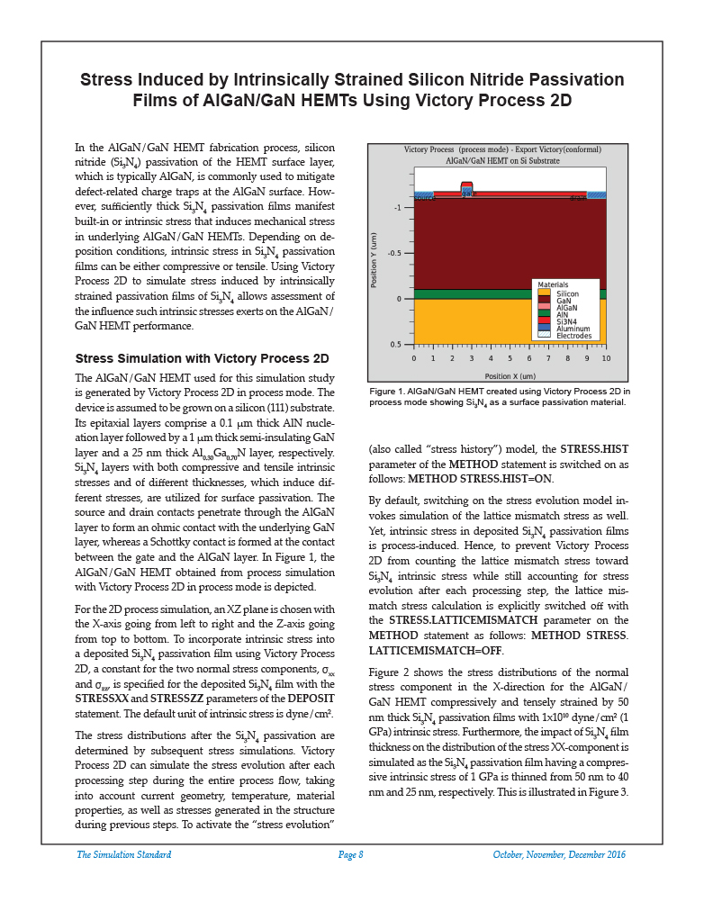
Stress Induced By Intrinsically Strained Silicon Nitride Passivation Films Of Algan Gan Hemts Using Victory Process 2d Silvaco
Review Of Gan Based Devices For Terahertz Operation

Sensors Free Full Text Algan Gan High Electron Mobility Transistor Based Biosensor For The Detection Of C Reactive Protein Html

Study Of Aln Gan Hemts 978 3 639 6 By Yu Cao
Kobra Uni Kassel De Bitstream Handle Dissertationsamirdahmani Pdf Sequence 3 Isallowed Y
Groove Type Channel Enhancement Mode Algan Gan Mis Hemt With Combined Polar And Nonpolar Algan Gan Heterostructures
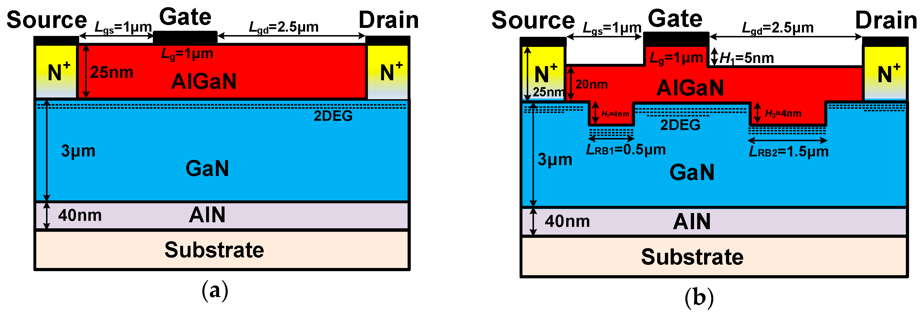
Micromachines Free Full Text Novel High Energy Efficiency Algan Gan Hemt With High Gate And Multi Recessed Buffer Html
Electronics Free Full Text A Comprehensive Review Of Recent Progress On Gan High Electron Mobility Transistors Devices Fabrication And Reliability Html
Gan Hemts Power Electric Motor Reform Mouser
Cuvillier De Uploads Preview Public File 7437 Pdf
Http Onlinelibrary Wiley Com Doi 10 1002 Pssc Pdf
Http Gaasmantech Com Digests 13 Papers 060 Pdf

Low Noise High Power Gan Hemt Technology For Manualzz
2
Http Publications Rwth chen De Record Files Javorka Peter Pdf
Pdfs Semanticscholar Org C221 Ed51d9ebc5811c9fdfde77a44dec9 Pdf

Cghv1j070d Datasheet Pdf Datasheet4u Com
Opus4 Kobv De Opus4 Btu Files 4598 Luo Peng Pdf


