Hemt Fabrication Process
Figure 31 Process workflow for fabrication and characterization 31 of HEMT mushroom gate structure Figure 32 Sample cleaning setup 34 Figure 33 Samco’s UV1 UV and Ozone Dry Stripper 35 Figure 34 A 10 x 10 array feature consisting gate test structures sets 36 Each set represents 10 strips of gate lines.
Hemt fabrication process. In this paper we demonstrate the possibility to fully integrate the process fabrication of RFMEMS switches in the GaNHEMT manufacturing steps to develop a RFMEMS/MMIC prototype MEMS RF performance reveals an insertion loss and an isolation respectively better than 06 dB and 25 dB in the frequency range 550 GHz. P330 ECS Journal of Solid State Science and Technology, 7 (6) P329P338 (18) improving performances47–50 Though, there is still a strong need to deeply investigate the influence of the thermal budget in order to orient and control the fabrication process Indeed, a precise knowledge. Currently GaN high electron mobility transistor (HEMT) technology is under extensive research in both industry and institutes Tinggi Technologies started to development its own HEMT process from 05 This paper evaluates the development of GaN HEMT in past 15 years and the entire fabrication process of Tinggi top GaN HEMT.
Process development of AlN/GaN MOSHEMTs is presented, along with issues and problems concerning the fabrication processes The developed technology uses thermally grown Al 2 O 3 as a gate dielectric and surface passivation for devices Significant improvement in device performance was observed using the following techniques (1) Ohmic contact optimisation using Al wet etch prior to Ohmic. GaN can be deposited on several types of substrates such as Sapphire, Silicon or Silicon Carbide (SiC), but the cost of GaN epi process and repeatable highquality crystal growth are challenges in GaNbased device fabrication. We can also provide device manufacturing and material analysis Foundry and material analysis services NTTAT also provides process services (including MEMS device prototyping, and etching services) and material analysis services InAlN HEMT structure Detailed specifications click here to download a leaflet of InAlN/GaN HEMT (PDF385KB).
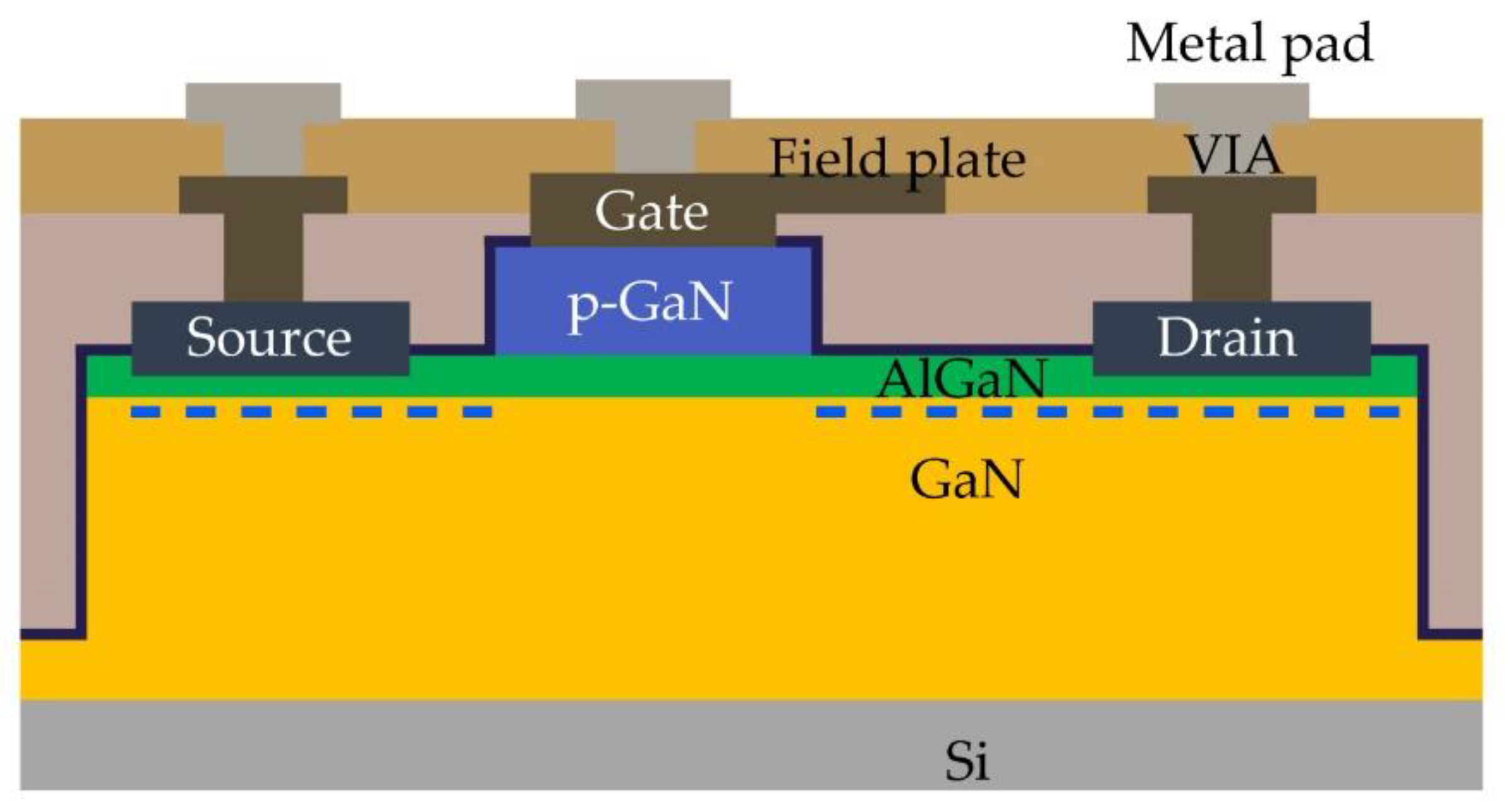
Infineon’s CoolGaN™ is a highly efficient GaN transistor technology for power conversion in the voltage range up to 600V With a longtime experience on the semiconductor market, Infineon brought the emode concept to maturity with endtoend production in high volumes. Fig 3 Flow chart of GaN HEMT fabrication process including field plate step After the passivation maximum current density was 1100 mA/mm and maximum extrinsic transconductance, g m was 260 mS/mm After this step, electron beam lithography is used to define the field plate regions and these regions were deposited with Ti/Au metals. The process modules for the GaN HEMT device fabrication include device isolation, pGaN gate formation, contacts for source and drain, contact for gate, surface passivation and so forth In this section, we will focus on some of the key process technologies for the fabrication of pGaN Emode AlGaN/GaN HEMTs, discuss some of the challenges and.
©17 by System Plus Consulting Panasonic PG6C09DV 24 Overview / Introduction Company Profile & Supply Chain Physical Analysis Manufacturing Process Flow Cost Analysis Selling Price Analysis Comparison o Transphorm, GaN System and Panasonic 600V GaN HEMT About System Plus Comparison between Transphorm, GaN System and Panasonic HEMT. Is the case with highvoltage devices A fabrication process flow has been developed for fabricating Schottkygate, and MISHEMT structures at UCF in the CREOL cleanroom The fabricated devices were designed to validate the simulation work for low voltage GaN devices The UCF fabrication process is done with a four layer mask, and consists of mesa. The epitaxial layers were grown on a 2in Si (111) substrate by MOCVD After the preparation of the epitaxial wafer, the normallyoff pGaN/AlGaN/GaN HEMT on a Si substrate was achieved by hydrogen plasma treatment The main structure of the epitaxial wafer includes a 1 µm GaN buffer layer, a 100 nm GaN channel layer, a 1 nm AlN spacer layer, an 18 nm undoped Al 02 Ga 08 N barrier layer.
GaN Transistor Fabrication Process With Liu Zhihong This chapter describes a few key process steps to fabricate GaN highelectronmobility transistors (HEMTs) for power electronics applications The whole process flow to fabricate a HEMT mainly includes five steps, namely mesa isolation, ohmic contact formation, gate formation, pad and. To increase the radiofrequency (RF) performance of AlGaN/GaNbased fintype high electron mobility transistors (HEMTs), a novel Tgate process was developed and applied to fabricate a device with high RF performance In a single lithography process, the applied Tgate process shows a technique for forming a Tgate using the reactivity difference of several photoresists The fabricated device. Fig 3 Flow chart of GaN HEMT fabrication process including field plate step After the passivation maximum current density was 1100 mA/mm and maximum extrinsic transconductance, g m was 260 mS/mm After this step, electron beam lithography is used to define the field plate regions and these regions were deposited with Ti/Au metals.
Figure 31 Process workflow for fabrication and characterization 31 of HEMT mushroom gate structure Figure 32 Sample cleaning setup 34 Figure 33 Samco’s UV1 UV and Ozone Dry Stripper 35 Figure 34 A 10 x 10 array feature consisting gate test structures sets 36 Each set represents 10 strips of gate lines. The fabrication steps of a pair of MetalOxideSemiconductor (MOS) Field Effect Transistor (FET) and a Bipolar Junction Transistor (BJT) on a Silicon wafer is illustrated in this applet The four buttons, 'first', 'previous', 'next', and 'last' let you view the static images at various points of the device fabrication. The HEMT device structure with OM picture is shown in Fig 2(a) In HEMT fabrication process, the source and drain terminal metal is deposited and then, diffused to the active layer by high temperature annealing But, the quality of metal contact often affects the basic switching characteristics.
Sheet Metal Fabrication has become the need of the 21st century as every industry you name, whether it is aircraft, railway, plumbing, manufacturing, or any other requires sheet metal to build products that can create a wave of technological advancement in the market The process of sheet metal fabrication involves turning flat sheets of aluminum or steel into metal structures by cutting. Metal fabrication is the creation of metal structures by cutting, bending and assembling processes It is a valueadded process involving the creation of machines, parts, and structures from various raw materials Typically, a fabrication shop bids on a job, usually based on engineering drawings, and if awarded the contract, builds the productLarge fab shops employ a multitude of valueadded. HEMT, the highest level of performance in the world could be realized with a signal gain of 16 dB and noise figure of 23–37dB with a size as small as 27 mm × 12 mm in the 3– GHz range Besides, a highoutputpower, compact size transceiver module was.
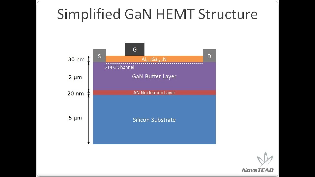
The HEMT structure consisted of a nm Al 025Ga 075N barrier layer on a 150nm GaN channel/buffer The twodimensional electron gas (2DEG) channel was formed near the GaN/AlGaN interface with 10x1013/cm2 carrier density, 15x10 3cm2/Vs mobility, and 450Ω/square sheet resistance The gatefirst fabrication process flow began with plasma. An average process sequence for a single device may contain –30 individual steps, some of which are considered to be the main steps of the process This main step receives greater attention during the development of a process document However, any set or combination of these steps may lead to a new technology. A new 650V GaN HEMT from Transphorm with a simplified cascode structure and enhanced electrical characteristics In tearing down the new TPH38PS GaN HEMT from Transphorm, System Plus Consulting has found the company is using a new manufacturing process.
The device fabrication technology is based on a mix and match approach by using both stepper and electron beam lithography The schematic of the circuit used for the doublechannel HEMT is shown in. Thus, an alternative approach is required in order to obtain improvement in the gate leakage In this study, we report a fabrication process of a normallyoff GaN MISHEMT with a gate leakage current as low as on the order of 10 −11 A/mm by exploiting a hydrofluoric (HF) acid pretreatment prior to gate formation 2. USA Fabrication of selfaligned, tgate hemt Google Patents Fabrication of selfaligned, tgate hemt Download PDF Info Publication number USA catabolic process Effects 0000 abstract description 4;.
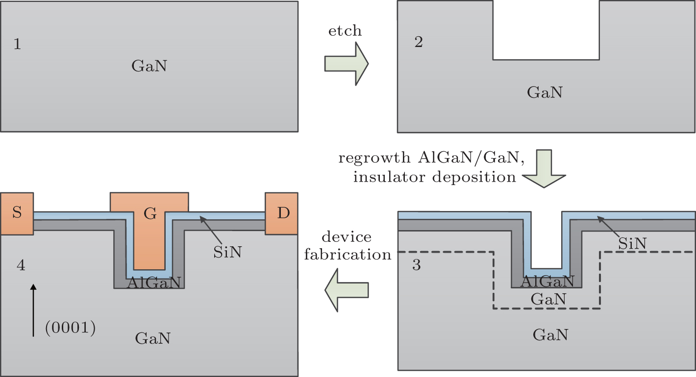
RFMEMS represent a feasible solution to obtain very low power dissipation and insertion loss, very high isolation and linearity switch respect to ldquosolid staterdquo technologies In this paper we demonstrate the possibility to fully integrate the process fabrication of RFMEMS switches in the GaNHEMT manufacturing steps to develop a RFMEMS/MMIC prototype. Request PDF New fabrication process to manufacture RFMEMS and HEMT on GaN/Si substrate RFMEMS represent a feasible solution to obtain very low power dissipation and insertion loss, very high. A GaNonSapphire HEMT Process Flow Example ③Deposit S/D metal Ø Deposit ohmic contacts on top of AlGaN as source and drain Sapphire Substrate Buffer GaN AlGaN S D ④Liftoff and Anneal Ø To improve contact quality Ø Bad annealing may dramatically degrade the device performance ⑤Mask 03 –Gate Ø Definegateregion Ø.
Northrop Grumman Space Technology (NGST) has recently initiated process development for fabricating 01 μm InGaAs/InAlAs/InP High Electron Mobility Transistor (HEMT) MMICs on 100 mm InP substrates Successful development of this process will further reduce costs for InP HEMT MMICs and rival those of GaAsbased HEMT MMICs, including GaAsbased metamorphic HEMT technology, with superior. His current research interests include the process development, fabrication and characterization of the GaAs psedomorphic HEMT, InP, and GaNbased HEMT devices for millimeter wave MMIC applications Mr Ji Heon Kim received the BS, MS, and Ph D degrees in department of electronics engineering from Chungnam National University, Daejeon. This is a list of semiconductor fabrication plantsA semiconductor fabrication plant is where integrated circuits (ICs), also known as microchips, are manufacturedThey are either operated by Integrated Device Manufacturers (IDMs) who design and manufacture ICs inhouse and may also manufacture designs from designonly (fabless firms), or by Pure Play foundries, that manufacture designs from.
FABRICATION, MODELING AND CHARACTERIZATION OF GaN HEMTs, AND DESIGN GaAs pHEMT process of UMS foundry We introduced twostage balanced PA GAN HIGH ELECTRON MOBILITY TRANSISTORS 8 21 GAN MATERIAL PROPERTIES8 22 PRINCIPLE OF GAN HEMT S. M S Cho et al Fabrication of AlGaN/GaN FinType HEMT Using a Novel TGate Process for Improved RF Performance FIGURE 3 IDSVGS transfer characteristics of the fabricated AlGaN/GaN fintype HEMT with a Tgate under VDS D 7 V The inset shows the IDSVGS transfer curves and gate leakage current on a logarithmic scale a gate to source length (LGS) of 6 m, and a gate to drain. Abstract We present a unique high yield, high performance 015 /spl mu/m HEMT production process which supports fabrication of MMW power MMICs up to 70 GHz This process has been transferred successfully from an R&D process to TRW's GaAs production line This paper reports the onwafer test results of more than 1300 Vband MMIC PA circuits measured over 24 wafers.
In this paper, we present a method for removing a high electron mobility transistor (HEMT) silicon substrate using mechanical grinding and deep silicon etching technology and successfully transferred the epitaxial wafer to a PET substrate to achieve the flexible normallyoff HEMT. A schematic of our fabrication process is sh own in Fig 2 Initially, HEMT devices are fabricated in serpentine geometries using our standard process shown in Fig 3a An Inductively Coupled Plasma (ICP) etch is then done to expose the Si substrate (Fig 3b) The sample is then mounted to glass slides using epoxy with. A generally Tshaped gate is formed by electron beam irradiation of a multilevel resist structure on a substrate The resist structure has an upper layer which is more sensitive to the electron beam than a lower layer thereof A generally Tshaped opening is formed in the resist structure by etching of the irradiated areas An electrically conductive metal is deposited to fill the opening and.
HEMT Manufacturing Process • HEMT Die FrontEnd Process • HEMT Die Fabrication Unit • Final Test and Packaging Fabrication Unit Cost Analysis • Overview of the Cost Analysis • Yield Explanations and Hypotheses • HEMT Die HEMT die frontend cost HEMT die probe test,. Al2O3 surface passivation and MOSgate fabrication on AlGaN/GaN highelectronmobility transistors without Al2O3 etching process JeongJin Kim1,2, YoungRak Park2, HyunGyu Jang2,3, JeHo Na 2, HyunSoo Lee4, SangChoon Ko , DongYun Jung 2, HyungSeok Lee , JaeKyoung Mun2,3, JingHong Lim 1, and JeonWook Yang * 1Department of Semiconductor Science and Technology/Semiconductor Physics. A key process in this study is dry etching In general, a Cl 2 based mixture gas is used to etch GaN15,16) In addition, to reduce damage from the etching, the inductively coupled plasma reactive ion etching (ICPRIE) technique is commonly applied17) For electrical isolation of the HEMT fabrication process in this study, ICP dry etching with.
2 Fabrication Fig 1 shows the crosssectional view of selfaligned Tgate AlGaN/GaN HEMT The epilayer of AlGaN/GaN HEMTstructure was grown by metalorganic chemical vapor deposition on (0001) sapphire substrate Theepilayer consists of40nmAINnucleation layer, 3,km of undoped GaN, and nmundoped Al03GaO7N The sheet resistance of. Microelectronic Engineering 19 (1992) 321 Elsevier Fabrication of 01pm planardoped pseudomorphic HEMT's using a PECVD silicon nitride assisted process G Zoua, W De Raedta, M Van Hovea, M Van Rossuma, Y Jinb, and H Launoisb aInteruniversity Microelectronics Center (IMEC vzw), 75 Kapeldreef, 001 Leuven, Belgium bL2M, CNRS, 196 Avenue Henri Rava, 922 Bagneux, France. A GaNonSapphire HEMT Process Flow Example ③Deposit S/D metal Ø Deposit ohmic contacts on top of AlGaN as source and drain Sapphire Substrate Buffer GaN AlGaN S D ④Liftoff and Anneal Ø To improve contact quality Ø Bad annealing may dramatically degrade the device performance ⑤Mask 03 –Gate Ø Definegateregion Ø.
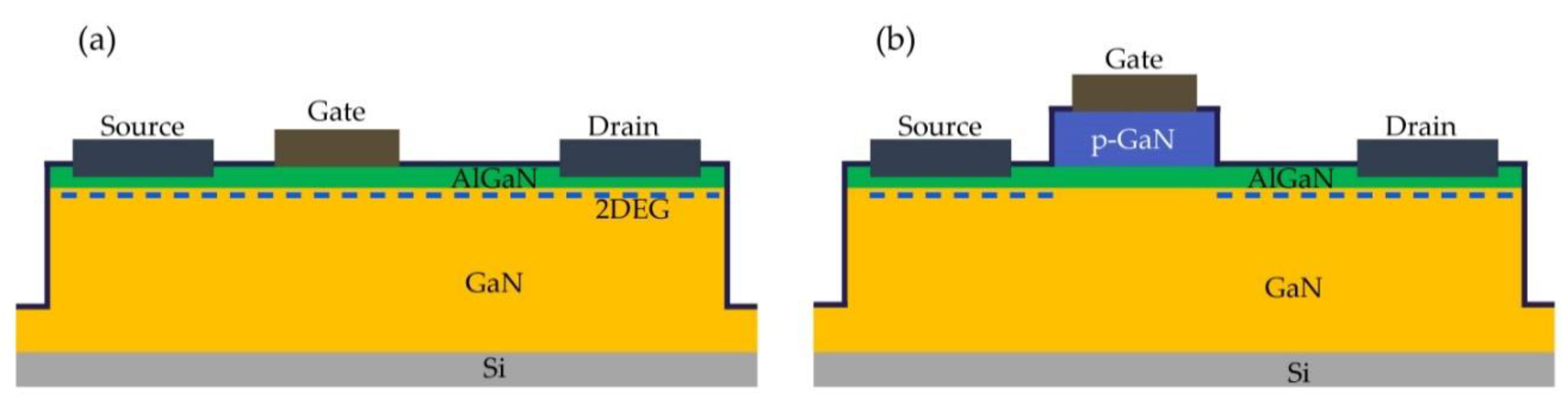
One of the challenges in GaN power device fabrication is to achieve a “normally off” operation While AlGaN/GaN High Electron Mobility Transistors (HEMT) devices are generally “normally on” and require a circuit to turn off the devices, a normallyoff operation is preferred for safety concerns. ©17 by System Plus Consulting Panasonic PG6C09DV 24 Overview / Introduction Company Profile & Supply Chain Physical Analysis Manufacturing Process Flow Cost Analysis Selling Price Analysis Comparison o Transphorm, GaN System and Panasonic 600V GaN HEMT About System Plus Comparison between Transphorm, GaN System and Panasonic HEMT. 2 Fabrication Fig 1 shows the crosssectional view of selfaligned Tgate AlGaN/GaN HEMT The epilayer of AlGaN/GaN HEMTstructure was grown by metalorganic chemical vapor deposition on (0001) sapphire substrate Theepilayer consists of40nmAINnucleation layer, 3,km of undoped GaN, and nmundoped Al03GaO7N The sheet resistance of.
Currently GaN high electron mobility transistor (HEMT) technology is under extensive research in both industry and institutes Tinggi Technologies started to development its own HEMT process from 05 This paper evaluates the development of GaN HEMT in past 15 years and the entire fabrication process of Tinggi top GaN HEMT. Fabrication HEMT has a fully equipped fabrication shop, capable to carry out fabrication of various types of process equipments like pressure vessel, heat exchangers, separator, columns etc We have expertise in fabrication of various types of structural works, water tanks, fixed type water tanks, diesel tank, frack tanks, etc. Prompted much research recently into the aluminium nitride/gallium nitride high electron mobility transistors (AlN/GaN HEMTs) in response to theoretical pre a protective layer is employed during fabrication of AlN/GaNbased devices However, in the presence of the protective/passivation layers, formation \New process for low sheet and.
Figure 31 Process workflow for fabrication and characterization 31 of HEMT mushroom gate structure Figure 32 Sample cleaning setup 34 Figure 33 Samco’s UV1 UV and Ozone Dry Stripper 35 Figure 34 A 10 x 10 array feature consisting gate test structures sets 36 Each set represents 10 strips of gate lines. 23 Fundamentals of AlGaN/GaN High Electron Mobility Transistors 23 231 AlGaN/GaN HEMT device structure and operating principles 24 232 Formation of 2DEG Channel due to Polarization Effect 27 CHAPTER 3 FABRICATION PROCESS AND CHARACTERIZATION. GaN HEMT devices are particularly significant in power electronics applications In this thesis, a comprehensive study of normallyoff highelectronmobility transistors is presented, including theoretical background review, theoretical analysis, physicallybased device simulations, device fabrication and optimization and.
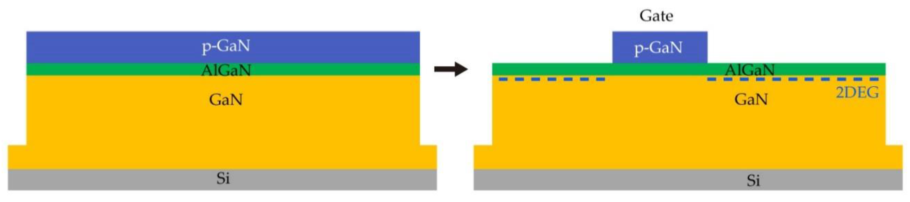
PGaN/AlGAN/GaN Emode HEMT Seungbin Jeong, Anand Lalwani March 22, 19 1 Members of the Project Fig5 gives us a summary of the whole fabrication process We prepare a silicon (111) wafer as the base substrate Then we grow the layers using MOCVD After that, we use 2 di erent masks for etching steps Fist,. Fig1 Schematic crosssection of fabricated AlGaN/GaN HEMT The fabrication process began with mesa isolation by Cl2/Ar electron cyclotron resonance reactive ion beam etching (ECRRIBE) After the mesaisolation, Ti/Al were evaporated by Ebeam and annealed by RTA in N2 ambient to form source and drain electrodes. M S Cho et al Fabrication of AlGaN/GaN FinType HEMT Using a Novel TGate Process for Improved RF Performance FIGURE 3 IDSVGS transfer characteristics of the fabricated AlGaN/GaN fintype HEMT with a Tgate under VDS D 7 V The inset shows the IDSVGS transfer curves and gate leakage current on a logarithmic scale a gate to source length (LGS) of 6 m, and a gate to drain.
Sheet Metal Fabrication has become the need of the 21st century as every industry you name, whether it is aircraft, railway, plumbing, manufacturing, or any other requires sheet metal to build products that can create a wave of technological advancement in the market The process of sheet metal fabrication involves turning flat sheets of aluminum or steel into metal structures by cutting. MESFET HEMT Oscillator – Wafer in Process Lecture 2 Fabrication Processes Wet EtchWet Etch Selectively remove material Chemical ProcessChemical Process Chemical Bath Patterned Photoresist Wafer in Process Lecture 2 Fabrication Processes MBE • Molecular Beam EpitaxyMolecular Beam Epitaxy. As development continues, GaN HEMT material growth and process development will be optimized so that the performance of the allSi foundry fabricated devices and circuits will be comparable to those fabricated in traditional IIIV foundries on Si.
Fabrication plan for Power HEMT using field plate Submitted By Vivek Kumar Surana Structure to be used 12 nm Al030Ga070N 10 nm Al2 Ga070 NSi nm Al030 Ga070N 030 1 nm AlN 140nm GaN 042m Al010Ga090N 70 nm Grad up to Al010 Ganm 70 AlN (HT) 090N 3 SiC STEP 1 SiNx passivation 300nm SiNx Technical parameters Deosited by ICPCVD SiH4/N2/Ar=28/9/90sccm Power 0W Pressure 35mTorr. The manufacture of an HEMT as follows procedure, first an intrinsic layer of Gallium Arsenide is set down on the semiinsulating Gallium Arsenide layer This is only about 1micron thick After that, a very thin layer between 30 and 60 Angstroms of intrinsic Aluminium Gallium Arsenide is set down on top of this layer.
2
Snfexfab Stanford Edu Sites G Files Sbiybj8726 F Sections Diplayfiles Engr241 Final Report Sj Al 1819win Pdf
Arxiv Org Pdf 1801
Hemt Fabrication Process のギャラリー
Analytical Model Development Of Channel Potential Electric Field Threshold Voltage And Drain Current For Gate Workfunction Engineered Short Channel E Mode N Polar Gan Mos Hemt Springerlink
Www Toshiba Co Jp Infrastructure En Defense Assets Pdf X Bandalganganhemtwithover80woutputpower Pdf
Transfer Printing And Self Aligned Etching For E Mode Gan Transistors
Http Publications Rwth chen De Record Files Javorka Peter Pdf
2
Www Osti Gov Servlets Purl
Comparing Gan On Sic Power Transistor Technology With Gaas And Si 5g Technology World
Www Ll Mit Edu Media 76

Beyond Cmos Heterogeneous Integration Of Iii V Devices Rf Mems And Other Dissimilar Materials Devices With Si Cmos To Create Intelligent Microsystems Philosophical Transactions Of The Royal Society A Mathematical Physical And Engineering
Groove Type Channel Enhancement Mode Algan Gan Mis Hemt With Combined Polar And Nonpolar Algan Gan Heterostructures
2
Http Www Cen Iitb Ac In Cen About Us Pdf Deliverable 4 Gan Pdf
Www Nature Com Articles S 019 3 Pdf Proof T
Www Csmantech Org Digests 04 04papers 4 3 Pdf
Avs Scitation Org Doi Am Pdf 10 1116 1
2

An Algan Gan Hemt By A Reversed Pyramidal Channel Layer Investigation And Fundamental Physics Sajjadi Jaghargh International Journal Of Numerical Modelling Electronic Networks Devices And Fields Wiley Online Library

Revisiting The Seminal Apa Optics Gan Hemt Patent Techinsights

Gan Power Devices The Hemt Youtube
Http Www Jkps Or Kr Journal Download Pdf Php Doi 10 3938 Jkps 59 439
2
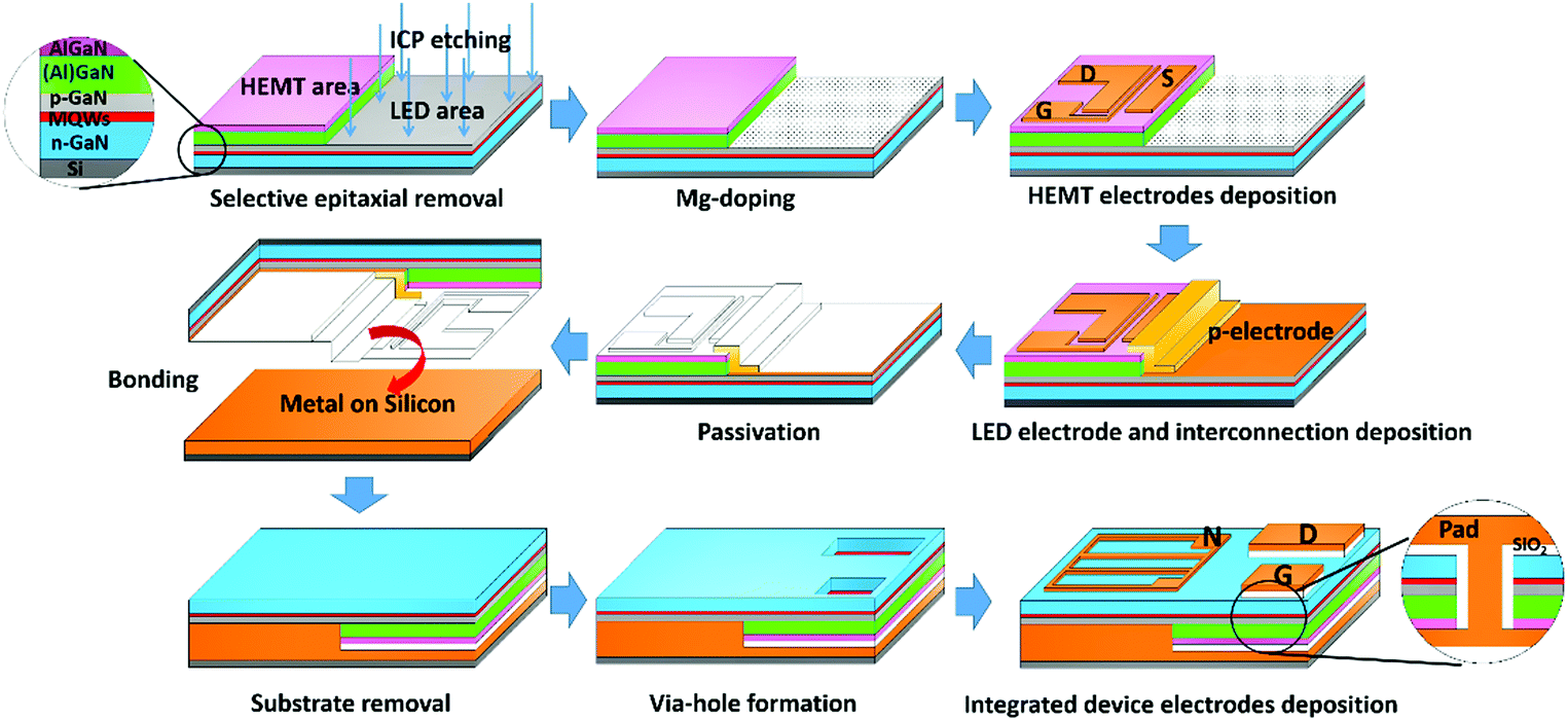
Efficiency Improved By Monolithic Integration Of Hemt With Vertical Structure Leds And Mg Doping On Dry Etched Gan Journal Of Materials Chemistry C Rsc Publishing Doi 10 1039 C9tch
Pure Tue Nl Ws Files 1 Pdf
Http Www Xidian Edu Cn Hyjsktz Docs Pdf
Http Trace Tennessee Edu Cgi Viewcontent Cgi Article 3211 Context Utk Graddiss

Sensors Free Full Text Algan Gan High Electron Mobility Transistor Based Biosensor For The Detection Of C Reactive Protein Html
Q Tbn And9gctpjmp Etncjaxg4vluiy0pdynte9s3v0fp3dfpb45jgr30c7cc Usqp Cau
Iopscience Iop Org Article 10 10 1361 6463 af9d Pdf
Www Tandfonline Com Doi Pdf 10 1080

Wolfspeed Rf Gan Hemt Cghvf I Micronews
Publikationen Bibliothek Kit Edu

Selective Epitaxial Growth Of Monolithically Integrated Gan Based Light Emitting Diodes With Algan Gan Driving Transistors Applied Physics Letters Vol 104 No 9
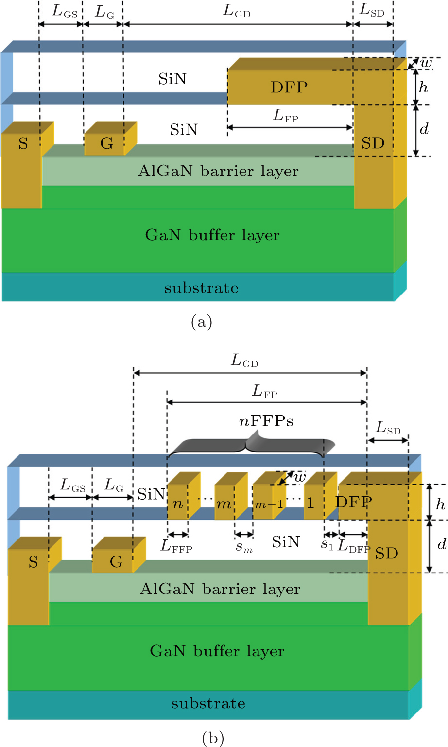
Reverse Blocking Characteristics And Mechanisms In Schottky Drain Algan Gan Hemt With A Drain Field Plate And Floating Field Plates
Http Etd Auburn Edu Bitstream Handle 4065 Ruocan Wang Ms Thesis Pdf Sequence 2 Isallowed Y
Http Userweb Eng Gla Ac Uk Mscposters14 15 Engineering and management Eee and management Developing of low Resistance ohmic contact on gan hemts Pdf
Http Www Ep Liu Se Ecp 008 Posters 008 Ecpp Pdf
2
Stars Library Ucf Edu Cgi Viewcontent Cgi Article 7690 Context Etd
2
Repository Asu Edu Attachments Content Tmp Package Mdb25d Guerra Asu 0010e Pdf
2

Fabrication Process Flow Of Gan Hemts With T Shape Gates Download Scientific Diagram
Gaasmantech Com Digests 10 Papers 11 2 056 Pdf
2
Electrical Characterization And Nanoscale Surface Morphology Of Optimized Ti Al Ta Au Ohmic Contacts For Algan Gan Hemt Topic Of Research Paper In Nano Technology Download Scholarly Article Pdf And Read For Free On Cyberleninka Open
Iopscience Iop Org Article 10 1149 2 jss Pdf
Www Armms Org Media Uploads Pdf
Tel Archives Ouvertes Fr Tel Document
Core Ac Uk Download Pdf Pdf

Efficiency Improved By Monolithic Integration Of Hemt With Vertical Structure Leds And Mg Doping On Dry Etched Gan Journal Of Materials Chemistry C Rsc Publishing Doi 10 1039 C9tch
2

Making Waves With The Gan Hemt News
Www Osti Gov Servlets Purl
2
2
Strain Balanced Algan Gan Algan Nanomembrane Hemts Scientific Reports

Moscap And Hemt Process Flows A Moscap Process Flow N Gan Substrate Download Scientific Diagram
2

High Performance Ultraviolet Light Detection Using Nano Scale Fin Isolation Algan Gan Heterostructures With Zno Nanorods Abstract Europe Pmc
Par Nsf Gov Servlets Purl

High Electron Mobility Transistors Hemt Ppt Video Online Download
Iopscience Iop Org Article 10 1149 1 Pdf
Gaasmantech Com Digests 03 03pdf 13 3 Pdf
2

Color Online Flowchart Of Backside Processing Of The Gan Hemt On A Download Scientific Diagram
Fabrication Process And A Schematic Diagram Of The Studied Sensors Download Scientific Diagram
Http Www Naun Org Main Naun Circuitssystemssignal 15 005 029 Pdf
Micromachines Free Full Text Novel High Energy Efficiency Algan Gan Hemt With High Gate And Multi Recessed Buffer Html
Core Ac Uk Download Pdf Pdf
Scholarcommons Sc Edu Cgi Viewcontent Cgi Article 4657 Context Etd
Gan Sic Based High Electron Mobility Transistors For Integrated Microwave And Power Circuits
Q Tbn And9gcr5yaa9idzub4ouuiyyzodc4vgznki8dmenjmdrrbhgxf9ysttf Usqp Cau
2
High Electron Mobility Transistor Wikipedia
Http Www Semiconductor Today Com Features Pdf Semiconductortoday Feb13 Step Towards Pdf

Beyond Cmos Heterogeneous Integration Of Iii V Devices Rf Mems And Other Dissimilar Materials Devices With Si Cmos To Create Intelligent Microsystems Philosophical Transactions Of The Royal Society A Mathematical Physical And Engineering
Arxiv Org Pdf 1905
Http Epubs Surrey Ac Uk 1 Pdf
Snfexfab Stanford Edu Sites G Files Sbiybj8726 F Sections Diplayfiles Engr241 Final Report Sj Al 1819win Pdf

Molecular Gated Algan Gan High Electron Mobility Transistor For Ph Detection Analyst Rsc Publishing
Electronics Free Full Text A Comprehensive Review Of Recent Progress On Gan High Electron Mobility Transistors Devices Fabrication And Reliability Html
Www Systemplus Fr Wp Content Uploads 19 06 Sp Infineon 600v Coolgan Transistor Family Flyer Pdf
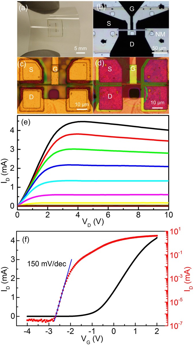
Nanoscalereslett Springeropen Com Track Pdf 10 1186 S 019 3025 8
Par Nsf Gov Servlets Purl

Low Noise High Power Gan Hemt Technology For Manualzz
Http Publications Rwth chen De Record Files Javorka Peter Pdf
2
Gan Sic Based High Electron Mobility Transistors For Integrated Microwave And Power Circuits
2
2
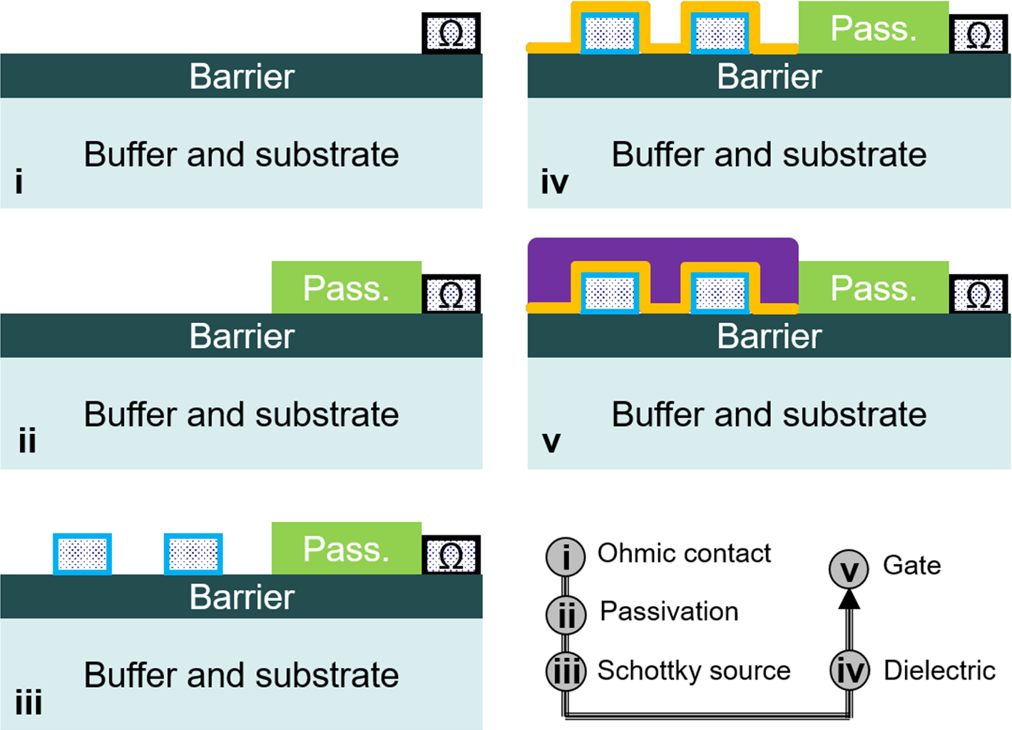
Figure 11 Proposal Of A Novel Recess Free Enhancement Mode Algan Gan Hemt With Field Assembled Structure A Simulation Study Springerlink

Pdf Development Of Advanced Technologies For The Fabrication Of Iii V High Electron Mobility Transistors Semantic Scholar
Electronics Free Full Text A Comprehensive Review Of Recent Progress On Gan High Electron Mobility Transistors Devices Fabrication And Reliability Html
Www Tu Ilmenau De Fileadmin Media Mne Nano Publikationen Jacobs Pssa214 Ic Algan Hemt Jatal Pdf
Electronics Free Full Text A Comprehensive Review Of Recent Progress On Gan High Electron Mobility Transistors Devices Fabrication And Reliability Html
2
Http Citeseerx Ist Psu Edu Viewdoc Download Jsessionid 992ceacdd061e25e7518bc6 Doi 10 1 1 651 4801 Rep Rep1 Type Pdf
Gan Hemt Power Device Tcad Simulation Youtube
Open Article In A Full Window


