Hemt Principle Of Operation
This book focusses on IIIV high electron mobility transistors (HEMTs) including basic physics, material used, fabrications details, modeling, simulation, and other important aspects It initiates by describing principle of operation, material systems and material technologies followed by description of the structure, IV characteristics, modeling of DC and RF parameters of AlGaN/GaN HEMTs.
Hemt principle of operation. 3 Highefficiency operation testing To evaluate efficiency in actual power electronics equipment, we mounted and evaluated a GaN HEMT on a power factor correction (PFC) circuit A schematic diagram of this singleswitch PFC circuit and a photo of the prototype PFC circuit are shown in Figures 3 (a) and (b), respectively In this circuit, the. The market of GaNbased HEMT power conversion devices is expected to be six hundred million dollars in 22 Features that set this work apart from similar achievements There are a number of distinctive features of HEMT as summarized below 1 Unique device operation principle and excellent fabrication technologies of HEMT. RF GaN HEMT devices Under normal operation all Wolfspeed GaN RF devices require a negative gate voltage and positive drain voltage for operation, with the gate voltage having to be applied first to prevent failure The bias sequencing circuit presented here uses a single DC power supply for both the gate and drain.
Layout is critical for paralleling high speed GaN HEMT Low and balanced parasitic inductance on the power and gate drive loop Equal length of gate drive layout and optimum gate driver circuit Summary Provided practical design guide on how to parallel high speed GaN HEMT devices. The first generation of 600 V GaN HEMT is intrinsically normally on device To easily apply normally on GaN HEMT in circuit design, a lowvoltage silicon MOSFET is in series to drive the GaN HEMT, which is well known as cascode structure This paper studies the characteristics and operation principles of a 600 V cascode GaN HEMT. A Junction FET The Junction FET transistor is a type of fieldeffect transistor that can be used as an electrically controlled switch The electric energy flows through an active channel between sources to drain terminals By applying a reverse bias voltage to the gate terminal, the channel is strained so the electric current is switched off completely.
Surprisingly little effort has been directed toward the study of sensor devices which involve the HEMT operation principle directly 6, 7 To demonstrate high sensitive and fast detection ability of the HEMT based sensor device at high operation temperatures, new high temperature stable Schottky gate absorption layers are needed. The basic structure and the principle of operation of HEMT’s have been presented in this Chapter HEMT is, perhaps, the quantum well device, which has found maximum applications as a lowsignal highgain and lownoise device, as well as a high power device upto microwave and millimeter wave frequencies The device, however, is of great interest to researchers. High Electron Mobility Transistor (HEMT) or Heterostructure FET (HFET) These transistors are characterized by a very high speed of operation and work on the principle of quantum tunneling InvertedT FET (ITFET) These have a part of the device vertically extending from the horizontal plane.
InPbased HEMT, GaNbased HEMT, modulationdoped superlattice, radio telescope 1 Introduction It has been more than 25 years since the high electron mobility transistor (HEMT) was first proposed in ) The key concept of the HEMT is the fieldeffect modulation of the highmobility twodimensional electron gas (2DEG). 3 HEMT basic 34 HEMT operation A high electron mobility transistor (HEMT) is a kind of a field effect transistor where the current flow between two ohmic contacts, source and drain, is controlled by a third contact, the gate which may be a Schottky barrier contact in most cases (1) Usually a field effect transistors channel is formed by a doped region as is generally the case for well known. The principle of operation of the HEMT is based on the properties of a high‐mobility two‐dimensional gas (2DEG) and high‐speed saturation channel of a 2DEG AlGaN HEMT is very close to the surface that is very sensitive to absorption of analytes We use this microsystem for detection of substances found in biological solutions.
Operation Principle and Structure of normallyoff Floating Gate GaN HEMT with Injection Gate Nagumo Kenshi, Kimoto Daiki, Suwa Tomoyuki (Tohoku Univ), Teramoto Akinobu (Hiroshima Univ), Shirota Riichiro, Tskatani Shinichiro , Kuroda Rihito, Sugawa Shigetoshi (Tohoku Univ) ED MW Abstract (in Japanese) (See Japanese page). HEMT Unique operation principle of the transistor enables unprecedented device characteristics suitable for efficient and linear millimeterwave power amplifier applications The lateral gate simultaneously modulate multiple 2DEG channels formed in an Al(Ga)N/GaN heterostructure A higher electron saturation. Since HEMTs and PHEMTs are fieldeffect transistors, the basic principles of their operation are very similar to those of the MESFET described in Section 3III The main difference between HEMTs and MESFETs is the epitaxial layer structure In the HEMT structure, compositionally different layers are grown in order to optimize and to.
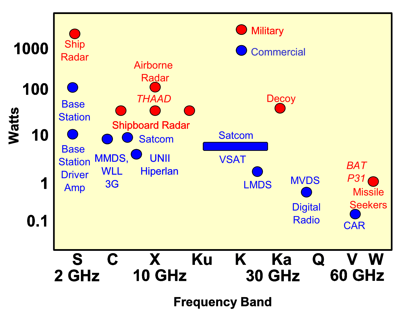
Operation Furthermore, the widebandgap offers a rugged and reliable technology capable of high voltagehigh temperature operation This opens up several industrial, automotive and aircraft applications like power and high voltage rectifiers and converters Some of the commercial and military markets that can be targeted by GaN are shown in. Performance, GaN HEMT can achieve 100W or higher with just a single device, making highefficiency and powersaving power amplification possible Recently, GaN HEMT R&D has been expanding to power conversion electronics Their operation frequency is less than several ten MHz in contrast to the GHz operation of highfrequency power amplifiers. The operation of the HEMT is a bit different to other types of FET and as a result, it is able to give a very much enhanced performance over the standard junction or MOS FETs, and in particular in microwave RF applications The electrons from the ntype region move through the crystal lattice and many remain close to the Heterojunction.
Because of the global trends of energy demand increase and decarbonization, developing green energy sources and increasing energy conversion efficiency are recently two of the most urgent topics in energy fields The requirements for power level and performance of converter systems are continuously growing for the fast development of modern technologies such as the Internet of things (IoT) and. Using HEMT (high electron mobilit y transistor) based heterostructures (AlGaN / GaN), it is possible to produce biological, chemical and medical sensors The principle of operation relies on the. HEMT operation The operation of the HEMT is somewhat different to other types of FET Electrons from the ntype region move through the crystal lattice and many remain close to the heterojunction These electrons form a layer that is only one electron thick forming what is known as a two dimensional electron gas.
A highelectronmobility transistor (HEMT), also known as heterostructure FET (HFET) or modulationdoped FET (MODFET), is a fieldeffect transistor incorporating a junction between two materials with different band gaps (ie a heterojunction) as the channel instead of a doped region (as is generally the case for a MOSFET)A commonly used material combination is GaAs with AlGaAs, though there. Operation Principle and Structure of normallyoff Floating Gate GaN HEMT with Injection Gate Nagumo Kenshi, Kimoto Daiki, Suwa Tomoyuki (Tohoku Univ), Teramoto Akinobu (Hiroshima Univ), Shirota Riichiro, Tskatani Shinichiro , Kuroda Rihito, Sugawa Shigetoshi (Tohoku Univ) ED MW Abstract (in Japanese) (See Japanese page). Maximum intrinsic frequency of operation for a HEMT device is directly proportional to the electron velocity Listed in Table 51 for comparison is the band gap energy (Eg), electron mobility (μe), peak velocity (vp), and lattice constant (a) for a number of important semiconductors Table 51.
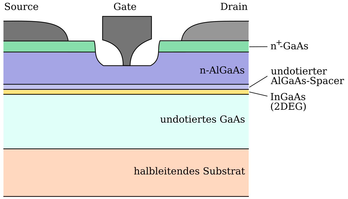
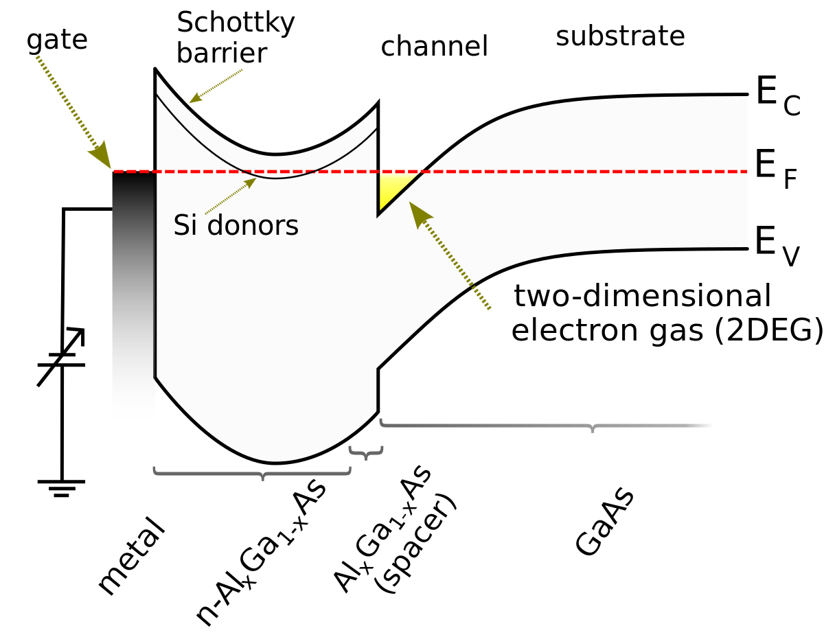
1 Unique device operation principle and excellent fabrication technologies of HEMT As mentioned previously, this was the world’s first transistor that used the field effect to control the density of electrons having high mobility. In recent years, high electron mobility transistors (HEMTs) have attracted much attention in highspeed and highpower The working principle of HEMT is described in section II Various HEMT versions and doped layer) does not participate in the conduction of any portion of the device operation Fig 2 Band energy diagram of HEMT. 2 The Principles of a HEMT HEMTs are field effect transistors where the current flow between two ohmic contacts, source and drain, is controlled by a third contact, the Most often the gate is a Schottky contact.
(AlGaN/GaN) High electron mobility transistors Low dimensional System Master of Nanoscience Olatz Idigoras Lertxundi Outline Introduction Gallium Nitrate AlGaN/GaN HEMT operation principles 2 dimensional electron gas Origin of 2 dimensional electron gas Charge control Summary References Introduction Transistor are used in many electronic devices, eg switch, amplifiers, oscillators. High Electron Mobility Transistors Presented by Date 04/28/14 SujanaKorrapati, SaiDivya Anne Abstract HEMT is a field effect transistor incorporating a junction between two materials with different band gaps as the channel We will discuss different types of HEMTs and their Applications. This book focusses on IIIV high electron mobility transistors (HEMTs) including basic physics, material used, fabrications details, modeling, simulation, and other important aspects It initiates by describing principle of operation, material systems and material technologies followed by description of the structure, IV characteristics.
HEMT operation The operation of the HEMT is somewhat different to other types of FET Electrons from the ntype region move through the crystal lattice and many remain close to the heterojunction These electrons form a layer that is only one electron thick forming what is known as a two dimensional electron gas. Principle and Working of JFET Principle of JEFT Fig3 shows the circuit of nchannel JFET with normal polarities The two pn junctions at the sides form two depletion layers The current conduction by charge carriers (ie electrons) is through the channel between the two depletion layers and out of the drain. In general, 600V GaN HEMT is intrinsically normallyon device To easily apply depletion mode GaN HEMT in circuit design, a low voltage silicon MOSFET is in series to drive the GaN HEMT, which is well known as cascode structure This paper studies the characteristics and operation principles of 600V cascode GaN HEMT.
InPbased HEMT, GaNbased HEMT, modulationdoped superlattice, radio telescope 1 Introduction It has been more than 25 years since the high electron mobility transistor (HEMT) was first proposed in ) The key concept of the HEMT is the fieldeffect modulation of the highmobility twodimensional electron gas (2DEG). In recent years, high electron mobility transistors (HEMTs) have received extensive attention for their superior electron transport ensuring high speed and high power applications HEMT devices are competing with and replacing traditional field‐effect transistors (FETs) with excellent performance at high frequency, improved power density and satisfactory efficiency. 2 The Principles of a HEMT HEMTs are field effect transistors where the current flow between two ohmic contacts, source and drain, is controlled by a third contact, the gate Most often the gate is a Schottky contact In contrast to ion implanted MESFETs HEMTs are based on epitaxially grown layers with different band gaps E g.
1 Unique device operation principle and excellent fabrication technologies of HEMT As mentioned previously, this was the world’s first transistor that used the field effect to control the density of electrons having high mobility. RBHEMT operation principle The back gate is biased in depletion to avoid conduction through the AlGaN layer, and RFsignal is fed to the back gate Schottky contact (Port 1) for launching acoustic wave 2DEG acts as the bottom electrode for acoustic excitation Thicknessmode resonance is. HEMT WORKING The operation of the HEMT is somewhat different to other types of FET and as a result it is able to give a very much improved performance over the standard junction or MOS FETs, and in particular in microwave radio applications.
(AlGaN/GaN) High electron mobility transistors Low dimensional System Master of Nanoscience Olatz Idigoras Lertxundi Outline Introduction Gallium Nitrate AlGaN/GaN HEMT operation principles 2 dimensional electron gas Origin of 2 dimensional electron gas Charge control Summary References Introduction Transistor are used in many electronic devices, eg switch, amplifiers, oscillators. The market of GaNbased HEMT power conversion devices is expected to be six hundred million dollars in 22 Features that set this work apart from similar achievements There are a number of distinctive features of HEMT as summarized below 1 Unique device operation principle and excellent fabrication technologies of HEMT. Of AlGaN/GaN High Electron Mobility Transistor (HEMT) using commercial software (Synopsys, Sentaurus TCAD) The model is calibrated against measurement data The results show a close matching with measured data, although some discrepancies have been found in the linear region of DC operation and high frequency regime of AC analysis.
3 HEMT basic 34 HEMT operation A high electron mobility transistor (HEMT) is a kind of a field effect transistor where the current flow between two ohmic contacts, source and drain, is controlled by a third contact, the gate which may be a Schottky barrier contact in most cases (1) Usually a field effect transistors channel is formed by a doped region as is generally the case for well known. GaN HEMT devices are particularly significant in power electronics applications In this thesis, a comprehensive study of normallyoff highelectronmobility transistors is presented, including theoretical background review, theoretical analysis, physicallybased device simulations, device fabrication and optimization and. Losses in the operation with a higher dv/dt slew rate The principle of the adaptive deadtime control is demonstrated in Figure 6 where the optimum dead time is almost equal to the switchnode capacitor charging time The optimum dead time is dependent on the inductor current and switch node capacitance and requires realtime correction in each.
•Overview of GaN HEMT Process and Device Simulation •Compact Modeling Standardization Effort two standard models (ASM, MVSG) •GaN HEMT Model Extraction for Symmetric and Asymmetric Devices •The MVSG model has a good geometry scalability in fitting devices with different gate lengths •TCAD simulations provides a unique approach to separate the extraction of temperature. Based on the operation principle, switch S1 and S2 work as freewheeling diode in the boost circuit s Large reverse recovery charge (Qrr) of existing silicon MOSFET makes the CCM operation of the totempole bridgeless PFC impractical, and reduces the total efficiency Table 1 gives a comparison of CoolMOS and GaN HEMT. GaN HEMT has attracted much attention as a candidate for SSPA devices because of its excellent capabilities such as high power, high efficiency and high gain with high voltage operation based on the excellent material properties of GaN In addition, the GaN HEMT is capable of covering wide bandwidth due to its high input and output impedance.
AlGaN/GaN HEMT has a special significant character, which creates two dimensional electron gases without doping process This attribute is mainly because of spontaneous polarization and the piezoelectric properties found in IIInitrides as shown in Fig 1These characteristics depend on the crystal structures of III nitrides. High Electron Mobility Transistors Presented by Date 04/28/14 SujanaKorrapati, SaiDivya Anne Abstract HEMT is a field effect transistor incorporating a junction between two materials with different band gaps as the channel We will discuss different types of HEMTs and their Applications. In general, 600V GaN HEMT is intrinsically normallyon device To easily apply depletion mode GaN HEMT in circuit design, a low voltage silicon MOSFET is in series to drive the GaN HEMT, which is well known as cascode structure This paper studies the characteristics and operation principles of 600V cascode GaN HEMT.
The formation of twodimensional electron gas (2DEG) in the quantum well is the main principle of the HEMT device operation and an analysis of unified n s for all regimes of device operation is a primary requirement in the development of a physics based compact model for these devices. The principle of operation of the HEMT is based on the properties of a highmobility twodimensional gas (2DEG) and highspeed saturation channel of a 2DEG AlGaN HEMT is very close to the surface. Operation can be achieved without passivation 2) The root cause of dispersion associated with surface states is often introduced during device processing;.
In particular, unintentional or unoptimized oxidation of the HEMT surface 3) These undesired surface states also lead to gate extension. InPbased HEMT, GaNbased HEMT, modulationdoped superlattice, radio telescope 1 Introduction It has been more than 25 years since the high electron mobility transistor (HEMT) was first proposed in ) The key concept of the HEMT is the fieldeffect modulation of the highmobility twodimensional electron gas (2DEG). This book focusses on IIIV high electron mobility transistors (HEMTs) including basic physics, material used, fabrications details, modeling, simulation, and other important aspects It initiates by describing principle of operation, material systems and material technologies followed by description of the structure, IV characteristics, modeling of DC and RF parameters of AlGaN/GaN HEMTs.
Depositonce Tu Berlin De Bitstream 8721 5 Badawi Nasser Pdf

Hemt Gan Docsity
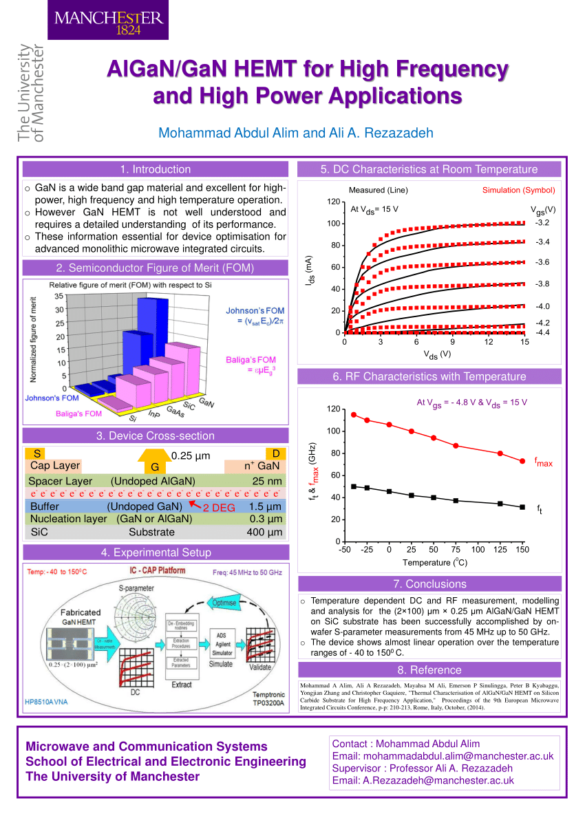
Pdf Algan Gan Hemt For High Frequency And High Power Applications
Hemt Principle Of Operation のギャラリー

Charge Conservative Gan Hemt Nonlinear Modeling From Non Isodynamic Multi Bias S Parameter Measurements International Journal Of Microwave And Wireless Technologies Cambridge Core
Www Mdpi Com 1996 1073 10 2 153 Pdf
Citeseerx Ist Psu Edu Viewdoc Download Doi 10 1 1 121 9375 Rep Rep1 Type Pdf
Www Theses Fr 17limo0084 Pdf
Http Trace Tennessee Edu Cgi Viewcontent Cgi Article 4269 Context Utk Graddiss
Nepp Nasa Gov Files G06jan I06mar Gan Tid Pdf
Nottingham Repository Worktribe Com Outputfile

Fluorine Plasma Surface Treatment For Gate Forward Leakage Current Reduction In Algan Gan Hemts
Etd Ohiolink Edu Apexprod Rws Etd Send File Send Accession Toledo Disposition Attachment
Scholarcommons Sc Edu Cgi Viewcontent Cgi Article 4657 Context Etd
Www Mouser Com Datasheet 2 692 Gsb Evbdb1 Userguide Rev Pdf
Http Www Nanoscience Gatech Edu Paper 1 S2 0 S Main Pdf
Cuvillier De Uploads Preview Public File Leseprobe Pdf
Publikationen Bibliothek Kit Edu

Current Trends In Changing The Channel In Mosfets By Iii V Semiconducting Nanostructures In Nanotechnology Reviews Volume 6 Issue 6 17
Arxiv Org Pdf 1102 4070
Linearity Aspects Of High Power Amplification In Gan Transistors Springerlink
Http Publications Rwth chen De Record Files Javorka Peter Pdf
Http Hig Diva Portal Org Smash Get Diva2 Fulltext01 Pdf

Gan Power Devices The Hemt Youtube
Http Oa Upm Es 1 Dejana Cucak Pdf
Charge Conservative Gan Hemt Nonlinear Modeling From Non Isodynamic Multi Bias S Parameter Measurements International Journal Of Microwave And Wireless Technologies Cambridge Core
2

Groove Type Channel Enhancement Mode Algan Gan Mis Hemt With Combined Polar And Nonpolar Algan Gan Heterostructures
Aip Scitation Org Doi Pdf 10 1063 1
Iopscience Iop Org Article 10 1149 2 jss Pdf
Groove Type Channel Enhancement Mode Algan Gan Mis Hemt With Combined Polar And Nonpolar Algan Gan Heterostructures
Http Www Ijirst Org Articles Ijirstv3i5040 Pdf
Gan Sic Based High Electron Mobility Transistors For Integrated Microwave And Power Circuits

Hemt Technology For High Speed Logic Communication Semiconductors Chemical Product Engineering
Pp Bme Hu Ee Article Viewfile 4558 3663
Www Mathmods Eu Resources Downloads Master Theses Finish 37 Master S Theses 262 Paul Ellinghaus Thesis
Ppt High Electron Mobility Transistors Powerpoint Presentation Free Download Id
Stars Library Ucf Edu Cgi Viewcontent Cgi Article 7690 Context Etd
Dspace Mit Edu Bitstream Handle 1721 1 Experimental characterization of thermal time constants manuscript Pdf Sequence 1 Isallowed Y
Tel Archives Ouvertes Fr Tel Document
Q Tbn And9gcr5yaa9idzub4ouuiyyzodc4vgznki8dmenjmdrrbhgxf9ysttf Usqp Cau
Sensors Free Full Text Investigation Of The Performance Of Hemt Based No No2 And Nh3 Exhaust Gas Sensors For Automotive Antipollution Systems Html
Http Publications Rwth chen De Record Files Javorka Peter Pdf
Micromachines Free Full Text A Novel Gan Metal Insulator Semiconductor High Electron Mobility Transistor Featuring Vertical Gate Structure Html

A A Schematic Thermal Electric Module B An Algan Gan Hemt Sensor Download Scientific Diagram
Http Download Xuebalib Com Xuebalib Com Pdf
Http Psrcentre Org Images Extraimages 30 7162 Pdf

High Electron Mobility Transistors Hemts Microwave Transistors And Tunnel Diodes Youtube
Www Nature Com Articles S 019 0106 6 Pdf Origin Ppub

Fluorine Plasma Surface Treatment For Gate Forward Leakage Current Reduction In Algan Gan Hemts
Depositonce Tu Berlin De Bitstream 8721 5 Badawi Nasser Pdf
2
2
Gan Sic Based High Electron Mobility Transistors For Integrated Microwave And Power Circuits

Functionalized Gan Based Transistors For Biosensing Intechopen
Q Tbn And9gcswoxpdcbljrdwesguh3iuarlzphuwhidhhhwit2yreb2obqblk Usqp Cau
Emission And Detection Of Terahertz Radiation Using Two Dimensional Plasmons In Semiconductor Nanoheterostructures For Nondestructive Evaluations
Www Osti Gov Pages Servlets Purl

High Electron Mobility Transistors Hemt Ppt Video Online Download

Gan Hemts The Benefits Of Far Higher Voltages News
Gan Sic Based High Electron Mobility Transistors For Integrated Microwave And Power Circuits

Pages From Physics Of Quantum Well Devices Solid State Science And Technology Library Field Effect Transistor Transistor
Gan Sic Based High Electron Mobility Transistors For Integrated Microwave And Power Circuits
Www Iitg Ac In Eee Vlsilab Pdf Iit guwahati august 17 Pdf
Gansystems Com Wp Content Uploads 18 10 A Full Power Emulation Platform For Evaluating Power Semiconductors Pdf
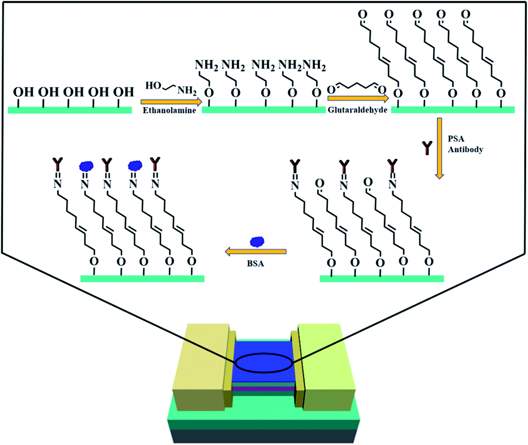
Highly Sensitive Algan Gan Hemt Biosensors Using An Ethanolamine Modification Strategy For Bioassay Applications Rsc Advances Rsc Publishing Doi 10 1039 C9ra055a
Www Ims Chips De Publication Exe Show Pdfbyid Php Study Thesis Report Alessandro Ottaviani Pdf Publicationid 1580 Doctyp 1 Redirect 1
Q Tbn And9gcss1v96r Q8ap10bshgpqpd99rlucff58gyjp3tzq8k6w5auzkp Usqp Cau

Functionalized Gan Based Transistors For Biosensing Intechopen
High Electron Mobility Transistor Wikipedia
Www Beam Verlag De App Download Hf Praxis 9 19 Iii Pdf
Ppt High Electron Mobility Transistors Powerpoint Presentation Free Download Id
Tel Archives Ouvertes Fr Tel Document
Kobra Uni Kassel De Bitstream Handle Dissertationsamirdahmani Pdf Sequence 3 Isallowed Y
Core Ac Uk Download Pdf Pdf
Opus4 Kobv De Opus4 Btu Files 4598 Luo Peng Pdf

Shows The Simulation Results Of Using The Gan Hemt The Modeling Download Scientific Diagram
Http Www Ejournal Org Cn Jweb Cje En Article Downloadarticlefile Do Attachtype Pdf Id 8581

An Algan Gan Hemt By A Reversed Pyramidal Channel Layer Investigation And Fundamental Physics Sajjadi Jaghargh International Journal Of Numerical Modelling Electronic Networks Devices And Fields Wiley Online Library
Aip Scitation Org Doi Pdf 10 1063 1

Gan Hemts The Benefits Of Far Higher Voltages News
Www Infineon Com Dgdl Infineon Cover Story Why Gan Is The Future For Class D Power Electronic News Ebook Article V01 00 En Pdf Fileid 5546dc0aeb6785d3035f
Www Osti Gov Pages Servlets Purl
High Electron Mobility Transistor Wikipedia

B

Sciencecentral
An Aunps Functionalized Algan Gan High Electron Mobility Transistor Sensor For Ultrasensitive Detection Of Tnt Rsc Advances Rsc Publishing
2
Characterization And Analysis Of Low Noise Gan Hemt Based Inverter Circuits Springerlink

Test Methods And Principles Of Thermal Resistance For Gan Hemt Power Devices Semantic Scholar
Http Publications Lib Chalmers Se Records Fulltext 5100 5100 Pdf
Www Db Thueringen De Servlets Mcrfilenodeservlet Dbt Derivate Ilm1 Pdf

An Algan Gan Hemt By A Reversed Pyramidal Channel Layer Investigation And Fundamental Physics Sajjadi Jaghargh International Journal Of Numerical Modelling Electronic Networks Devices And Fields Wiley Online Library
Repository Asu Edu Attachments Content Tmp Package Mdb25d Guerra Asu 0010e Pdf
Www Infineon Com Dgdl Infineon Cover Story Why Gan Is The Future For Class D Power Electronic News Ebook Article V01 00 En Pdf Fileid 5546dc0aeb6785d3035f

High Electron Mobility Transistors Hemt Ppt Video Online Download
Www Awr Com Serve M Gan Hemt
Operation Mechanism Of Gan Based Transistors Elucidated By Element Specific X Ray Nanospectroscopy Scientific Reports
Http Publications Rwth chen De Record Files Javorka Peter Pdf
Q Tbn And9gcsjzba15lyr9pfjlcss6ds6sztpovnicwekjqarzdbgy8gdpgf1 Usqp Cau
Improving The Transconductance Flatness Of Inaln Gan Hemt By Modulating Vt Along The Gate Width Iopscience
Par Nsf Gov Servlets Purl
Electronics Free Full Text A Comprehensive Review Of Recent Progress On Gan High Electron Mobility Transistors Devices Fabrication And Reliability Html

High Electron Mobility Transistors Hemt Ppt Video Online Download
Http Ieeexplore Ieee Org Iel7 16 Pdf


